Novel quantum well barrier layer LED epitaxial growth method and epitaxial layer

A technology of epitaxial growth and barrier layer, applied in electrical components, circuits, semiconductor devices, etc., can solve problems such as reducing internal quantum efficiency

Inactive Publication Date: 2014-11-19
XIANGNENG HUALEI OPTOELECTRONICS
View PDF6 Cites 22 Cited by
  • Summary
  • Abstract
  • Description
  • Claims
  • Application Information

AI Technical Summary

Problems solved by technology

After the current is injected, the electrons in the n-type GaN layer will easily pass through the light-emitting layer (active layer MQW) due to their high mobility,

Method used


Image

  • Novel quantum well barrier layer LED epitaxial growth method and epitaxial layer
  • Novel quantum well barrier layer LED epitaxial growth method and epitaxial layer
  • Novel quantum well barrier layer LED epitaxial growth method and epitaxial layer

Examples


Example Embodiment

[0052] Example one

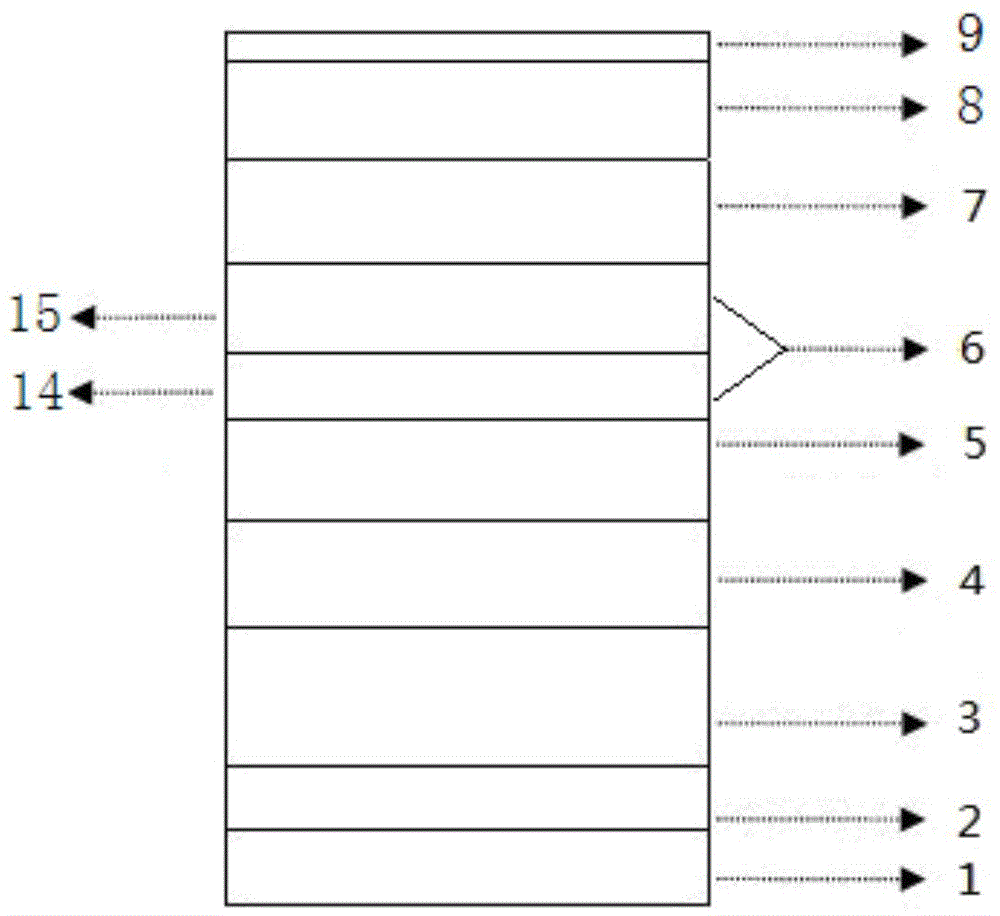
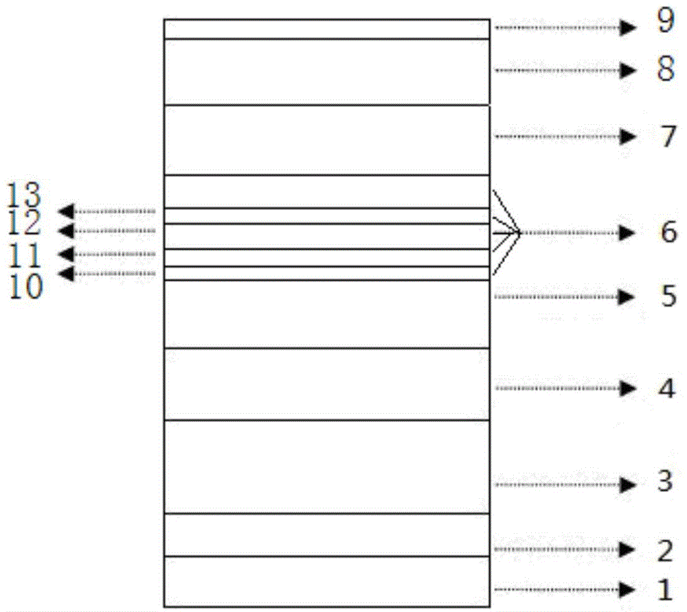
[0053] See figure 2 The present invention uses Aixtron MOCVD to grow high-brightness GaN-based LED epitaxial wafers. Using high purity H 2 Or high purity N 2 Or high purity H 2 And high purity N 2 Mixed gas as carrier gas, high purity NH 3 As the N source, metal organic source trimethylgallium (TMGa) and triethylgallium (TEGa) are used as the gallium source, trimethylindium (TMIn) is used as the indium source, and the N-type dopant is silane (SiH 4 ), trimethyl aluminum (TMAl) is used as the aluminum source, and the P-type dopant is magnesium cerocene (CP 2 Mg), the substrate is (0001) sapphire, and the reaction pressure is between 100mbar and 800mbar.

[0054] A new type of LED epitaxial growth method of quantum well barrier layer, including processing the substrate, growing a low-temperature buffer GaN layer, growing an undoped GaN layer, growing a Si-doped GaN layer, growing an active layer MQW, and growing P-type AlInGaN The steps of layering and growing a...


PUM

PropertyMeasurementUnit
Thicknessaaaaaaaaaa
Thicknessaaaaaaaaaa
Thicknessaaaaaaaaaa

Abstract

The invention provides a novel quantum well barrier layer LED epitaxial growth method and an LED epitaxial layer. The method sequentially comprises steps of processing a substrate, growing a low-temperature buffer GaN layer, growing a non-doped GaN layer, growing an n-type AlGaN layer, growing an n-type GaN layer, growing an active layer MQW, growing a P-type AlGaN layer, growing a P-type GaN layer and growing a p-type contact layer. the AlGaN thin layer is grown in a penetrating mode in the middle of the traditional active layer GaN barrier layer, the limiting and expanding ability of the light-emitting layer on electron can be enhanced, the ability of the quantum well to bond electron can be improved, the radiative recombination rate of a hole and electron in the potential well is obviously improved, the internal quantum efficiency is enhanced, and photoelectric properties of the LED device are improved.

Description

Technical field [0001] The present invention relates to the technical field of LED epitaxial design, in particular to a method for LED epitaxial growth of a novel quantum well barrier layer and an LED epitaxial layer. Background technique [0002] LEDs are widely used in a wide range of fields such as displays, sensors, communications, and lighting. As a core semiconductor device, GaN-based blue LEDs can be combined with phosphors to produce white light, which is very attractive in terms of lighting. [0003] To improve the luminous efficiency of LED epitaxial wafers, the most fundamental way is to enhance the internal quantum efficiency of the epitaxial structure. At present, the internal quantum efficiency of domestic MOCVD-grown GaN-based LED epitaxial wafers can only reach about 30%, and there is still much room for development and improvement. The growth of the active layer MQW is particularly important for the improvement of internal quantum efficiency. [0004] Currently, th...

Claims


Application Information

Patent Timeline
IPC IPC(8): H01L33/00H01L33/14H01L33/02
CPCH01L33/0075H01L21/0254H01L21/0262H01L33/06H01L33/14
Inventor 王霄梁智勇季辉
Owner XIANGNENG HUALEI OPTOELECTRONICS
Why Eureka
Try Eureka