Light-emitting diode epitaxial growth method

A technology of light-emitting diodes and epitaxial growth, applied in electrical components, circuits, semiconductor devices, etc., can solve the problems of uneven wavelength distribution, poor quality of LEDs, etc., to reduce testing and sorting costs, improve warpage, and improve uniformity. sexual effect

Active Publication Date: 2014-11-19
EPITOP PHOTOELECTRIC TECH
View PDF5 Cites 14 Cited by
  • Summary
  • Abstract
  • Description
  • Claims
  • Application Information

AI Technical Summary

Problems solved by technology

[0005] An embodiment of the present invention provides a light-emitting diode epitaxial growth method to overcome the problem of poor LED quality due to uneven wavelength distribution in epitaxy in the prior art

Method used


Image

  • Light-emitting diode epitaxial growth method
  • Light-emitting diode epitaxial growth method
  • Light-emitting diode epitaxial growth method

Examples


Embodiment Construction

[0026] In order to make the purpose, technical solutions and advantages of the embodiments of the present invention clearer, the technical solutions in the embodiments of the present invention will be clearly and completely described below in conjunction with the drawings in the embodiments of the present invention. Obviously, the described embodiments It is a part of embodiments of the present invention, but not all embodiments. Based on the embodiments of the present invention, all other embodiments obtained by persons of ordinary skill in the art without making creative efforts belong to the protection scope of the present invention.

[0027] The technical solution of the present invention will be described in further detail below through specific embodiments and accompanying drawings.

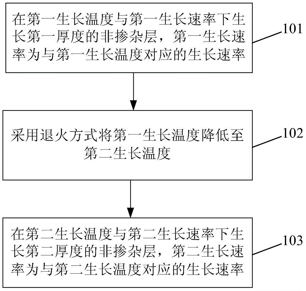
[0028] An embodiment of the present invention provides a method for epitaxial growth of a light emitting diode, and the method may specifically include:

[0029] On the substrate, a buffer...


PUM


Abstract

The invention provides a light-emitting diode epitaxial growth method. The method comprises the steps that a buffer layer, a non-doping layer, an N-type doping layer, a quantum well light-emitting layer and a P-type doping layer are sequentially grown on a substrate from bottom to top; the non-doping layer grows through the mode that the annealing process and adjustment on growth environment in a reaction chamber are performed alternatively; the growth environment comprises the growth temperature and the growth rate. The non-doping layer grows through the growth mode that the annealing process and the adjustment on the growth temperature and the growth rate of the non-doping layer in the reaction chamber are carried out alternatively, the epitaxial warping degree at the high temperature can be effectively improved, and therefore the epitaxial wavelength distribution evenness and LED quality can be improved. Further, the test and sorting cost can be reduced.

Description

technical field [0001] The invention relates to the technical field of semiconductors, in particular to an epitaxial growth method of a light emitting diode. Background technique [0002] The uniformity of the epitaxial wavelength of the light-emitting diode has an important impact on the performance of the light-emitting diode, and the doping amount of indium In, a component that plays a key role in wavelength adjustment, in the quantum well (InxGa1-xN) is very sensitive to temperature, and the temperature at 1 °C The temperature change will cause the light emitting diode (Light Emitting Diode, referred to as LED) wavelength drift of 3-5nm, and when the quantum well is grown at about 760 ℃, a slight change in the warpage will cause the temperature in the epitaxy to have 2-3 The change of ℃ will deepen the degree of LED wavelength drift. [0003] In the prior art, when metal-organic chemical vapor deposition (MOCVD) is used to grow LED epitaxy, there will be a certain latti...

Claims


Application Information

Patent Timeline
Patent Type & Authority Applications(China)
IPC IPC(8): H01L33/00
CPCH01L33/007H01L33/12
Inventor 焦建军黄炳源周德保康建梁旭东
Owner EPITOP PHOTOELECTRIC TECH
Why Eureka
Try Eureka