Thin-film transistor, manufacturing method of thin-film transistor, array substrate and display device

A technology of thin film transistors and substrate substrates, which is applied in transistors, semiconductor/solid-state device manufacturing, electric solid-state devices, etc., can solve the problem of increased subthreshold swing of thin film transistors, affecting the semiconductor characteristics of thin film transistors, reducing nitrogen vacancy mobility, etc. problem, achieve the effect of reducing subthreshold swing, improving semiconductor characteristics, and improving mobility

Active Publication Date: 2014-11-26
BOE TECH GRP CO LTD
View PDF4 Cites 5 Cited by
  • Summary
  • Abstract
  • Description
  • Claims
  • Application Information

AI Technical Summary

Problems solved by technology

[0005] However, the different content of nitrogen element in the ZnON material forming the active region will lead to different mobility, and in the conduction process of the thin film transistor and the ITO (indium tin oxide) of the display substrate (such as the array substrate) of the display device During the annealing process, the nitrogen element in the active re

Method used


Image

  • Thin-film transistor, manufacturing method of thin-film transistor, array substrate and display device
  • Thin-film transistor, manufacturing method of thin-film transistor, array substrate and display device
  • Thin-film transistor, manufacturing method of thin-film transistor, array substrate and display device

Examples


Embodiment 1

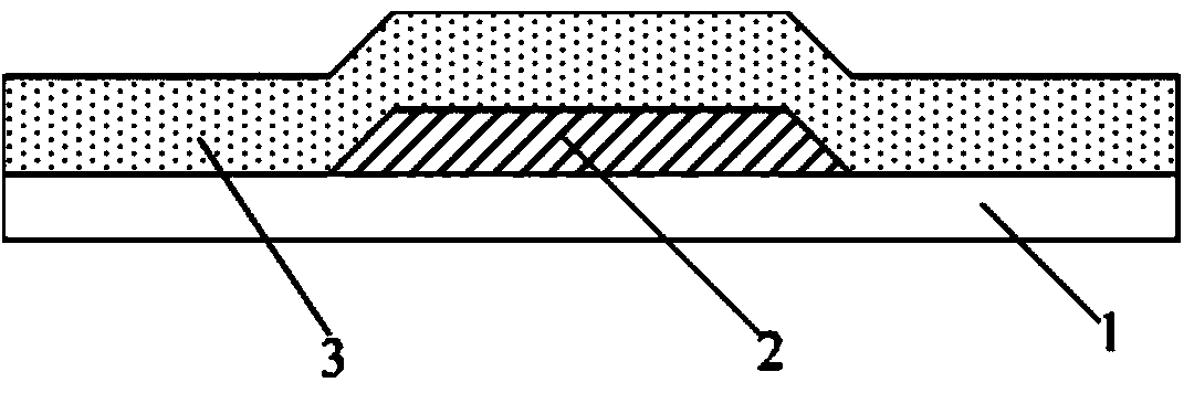
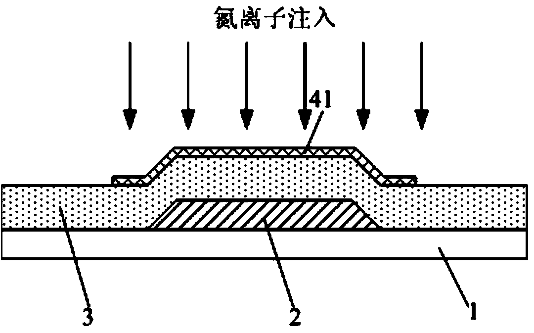
[0032] This embodiment provides a method for preparing a thin film transistor, such as Figure 1-6 As shown, it includes forming a gate 2, a gate insulating layer 3, an active region 4, a source 5 and a drain 6 on a base substrate 1, and the active region 4 is formed by using ZnON material, while forming the active region 4 Nitrogen ion implantation is performed on the active region 4 so that the sub-threshold swing of the thin film transistor is ≤0.5mV / dec.

[0033] Among them, the sub-threshold swing is the slope of the part of the semiconductor output characteristic curve from the off state (off state) to the on state (conducting state). The smaller the slope, the response of the thin film transistor from the off state to the on state The faster the speed, correspondingly, the better the subthreshold swing characteristics, and the better the performance of the thin film transistor; the larger the slope, the slower the response speed of the thin film transistor from the off ...

Embodiment 2

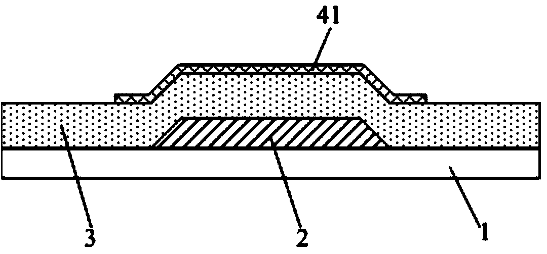
[0046] This embodiment provides a method for manufacturing a thin film transistor. The difference from Embodiment 1 is that the gate is formed above the active region, that is, the thin film transistor in this embodiment has a top-gate structure.

[0047] The preparation method of other structures of the thin film transistor in this embodiment is the same as that in Embodiment 1, and will not be repeated here.

[0048] Beneficial effects of embodiment 1-2: in the preparation method of the thin film transistor provided in embodiment 1-2, nitrogen ion implantation is performed on the active region while forming the active region, so that the active region is in an effective conductive position The concentration of nitrogen ions is greatly increased, so that when the thin film transistor is in the working state, the nitrogen element lost due to the diffusion effect in the active region can be sufficiently replenished, thereby greatly improving the mobility of nitrogen vacancies in...

Embodiment 3

[0050] This embodiment provides a thin film transistor, which is manufactured by any one of the preparation methods in Embodiments 1-2.

[0051] In this embodiment, the active region of the thin film transistor includes a first active region layer and a second active region layer, the second active region layer is located on the first active region layer, and the first active region layer is located The concentration of nitrogen ions at the effective conduction position is greater than the concentration of nitrogen ions at the effective conduction position in the second active region layer. Such setting can make the nitrogen ions in the first active region layer replenish into the second active region layer during the operation of the thin film transistor, and be in an effective conductive position in the second active region layer, thereby improving the The mobility of nitrogen vacancies in the entire active region further increases the mobility of carriers in the active regi...


PUM


Abstract

The invention provides a thin-film transistor, a manufacturing method of the thin-film transistor, an array substrate and a display device. The manufacturing method of the thin-film transistor comprises the steps that a grid, a gate insulator, an active area, a source and a drain are formed on the substrate, the active area is made of a ZnON material, and nitrogen ions are implanted in the active area while the active area is formed, so that the subthreshold swing of the thin-film transistor is smaller than or equal to 0.5 mV/dec. According to the manufacturing method, as the nitrogen ions are implanted in the active area while the active area is formed, the concentration of the nitrogen ions, at the effective electricity conducting position, in the active area can be greatly improved, when the thin-film transistor works, nitrogen, lost due to the diffusion effect, in the active area can be supplemented sufficiently, the migration rate of nitrogen vacancy in the active area can be greatly increased, namely, the migration rate of current carriers in the active area is greatly increased, the subthreshold swing of the thin-film transistor is further reduced, and the semi-conductor property of the thin-film transistor is improved.

Description

technical field [0001] The present invention relates to the field of display technology, in particular, to a thin film transistor, a manufacturing method thereof, an array substrate and a display device. Background technique [0002] Thin film transistors (TFTs) have been widely used in flat panel display devices due to their good switching characteristics. [0003] Generally, a thin film transistor includes a gate, an active region, a source and a drain, and the source and the drain are respectively arranged at two ends of the active region and are respectively in contact with the active region. When the gate voltage is higher than its threshold voltage, the source and drain conduct through the active region, and carriers flow from source to drain or from drain to source. [0004] The active region of thin film transistors can currently use ZnON (zinc oxynitride) materials. During the conduction process of ZnON materials, the nitrogen vacancies in them have high mobility, ...

Claims


Application Information

Patent Timeline
IPC IPC(8): H01L29/786H01L21/425H01L27/12
CPCH01L29/7869H01L21/02565H01L21/425H01L21/441H01L21/76829H01L21/76877H01L23/5226H01L27/1225H01L27/124H01L27/127H01L29/0684H01L29/24H01L29/66969H01L29/78696H01L2924/0002H01L2924/00H01L29/66742H01L21/26513H01L27/1214
Inventor 姜春生辛龙宝
Owner BOE TECH GRP CO LTD
Why Eureka
Try Eureka