Method for preparing surface micro-nano pattern by two-step method

A micro-nano and graphic technology, applied in welding equipment, manufacturing tools, laser welding equipment, etc., can solve the problems of difficult to realize complex pattern preparation, difficult placement of micro-fiber, etc., to achieve strong controllability and improved resolution. Effect

Active Publication Date: 2016-09-21
TSINGHUA UNIV
View PDF7 Cites 0 Cited by
  • Summary
  • Abstract
  • Description
  • Claims
  • Application Information

AI Technical Summary

Problems solved by technology

Although the optical fiber focusing method can obtain the effect of the near-field effect, it is difficult to realize the preparation of complex patterns due to the difficulty of placing the micro-fiber in the near-field region of the surface, and the prepared surface patterns are mostly linear.

Method used


Image

  • Method for preparing surface micro-nano pattern by two-step method
  • Method for preparing surface micro-nano pattern by two-step method
  • Method for preparing surface micro-nano pattern by two-step method

Examples


Embodiment 1

[0040] Example 1. Preparation of micro-nano patterns on the surface of polysilicon using femtosecond laser

[0041] 1. Using the femtosecond laser multiphoton polymerization processing method, the focusing element is prepared on the surface of polysilicon according to the required pattern requirements

[0042](1) Select polysilicon as the material to be processed, and uniformly coat IP-L photoresist (purchased from Nanoscribe, Germany) in the central area of ​​its surface. The characteristic absorption band of IP-L photoresist is 180nm-320nm.

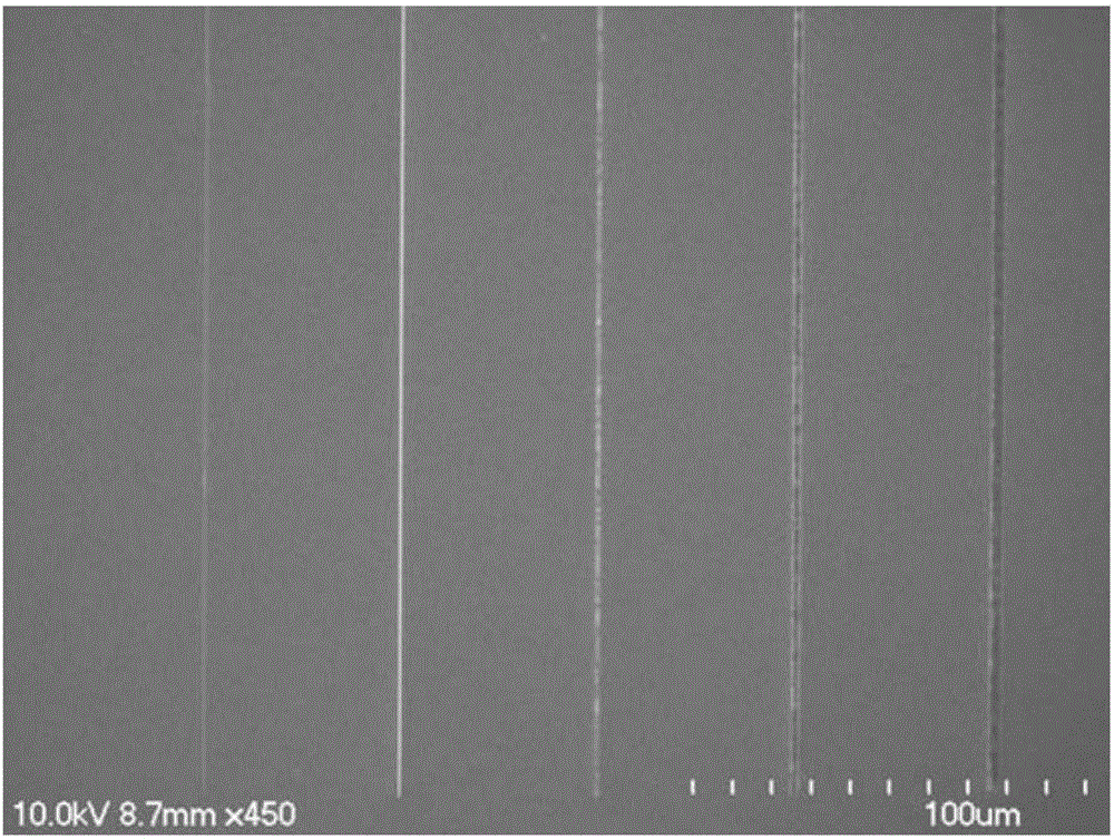
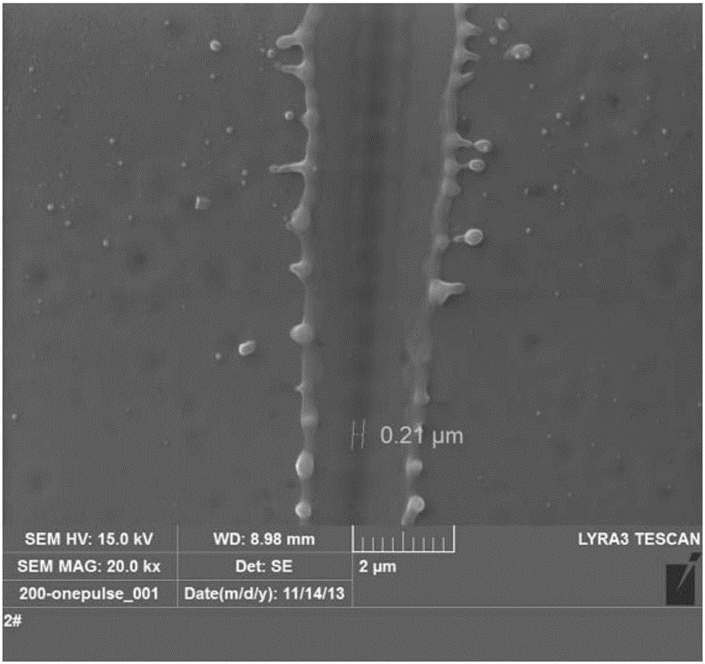
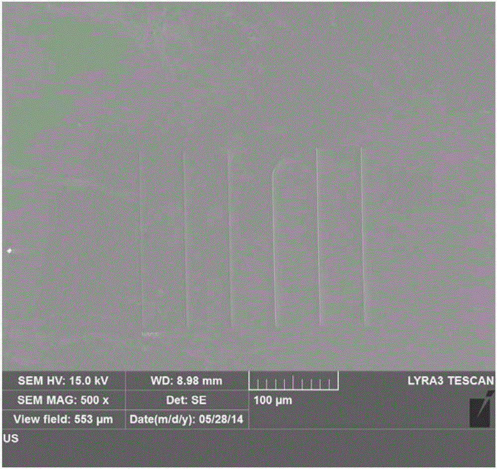
[0043] (2) According to requirements, strip trenches of different widths are to be prepared on the surface of polysilicon. Through calculation (the specific calculation method is as follows: use the finite difference time domain algorithm (FDTD) to calculate the energy field distribution of cylindrical polymeric components with different widths and diameters under the action of the laser, and compare it with the material damage threshol...

Embodiment 2

[0054] Example 2. Using nanosecond laser to prepare micro-nano patterns on the surface of polysilicon

[0055] 1. Using the femtosecond laser multiphoton polymerization processing method, the focusing element is prepared on the surface of polysilicon according to the required pattern requirements

[0056] (1) Select polysilicon as the material to be processed, and uniformly coat IP-L photoresist (purchased from Nanoscribe, Germany) in the central area of ​​its surface. The characteristic absorption band of IP-L photoresist is 180nm-320nm.

[0057] (2) According to requirements, strip trenches of different widths are to be prepared on the surface of polysilicon. Through calculation (the specific calculation method is as follows: use the finite difference time domain algorithm (FDTD) to calculate the energy field distribution of cylindrical polymeric components with different widths and diameters under the action of the laser, and compare it with the material damage threshold to...


PUM

PropertyMeasurementUnit
diameteraaaaaaaaaa
lengthaaaaaaaaaa
widthaaaaaaaaaa

Abstract

The invention discloses a method for preparing a surface micro-nano figure through two steps. The method comprises the following steps: (1), coating a processing region on the surface of a to-be-processed material with a photosensitive polymeric material; (2), according to a micro-nano figure prepared on the surface of the to-be-processed material, designing the shape of a focusing element, performing multiphoton polymerization processing on photosensitive polymeric material through a femtosecond laser multiphoton polymerization processing device; (3), performing laser radiation on the focusing element through the laser processing device of the surface micro-nano figure, namely obtaining the micro-nano figure on the surface of the to-be-processed material. The method has the advantages as follows: the preparation process is simple and convenient, and the resolution ratio in focusing processing process is increased, so that the preparation of the surface submicron-nano figures is realized; the laser multiphoton polymerization processing method is adopted, so that three-dimensional structures with all shapes can be prepared on the surfaces of all solid materials, therefore, the method can be widely applied to preparation of micro-nano figures with complex surfaces and can realize the preparation of large-area surface micro-nano figures.

Description

technical field [0001] The invention relates to a method for preparing surface micro-nano patterns by a two-step method, and belongs to the technical field of laser surface processing. Background technique [0002] The surface properties of materials, such as friction, wear, lubrication, and adhesion, mainly depend on the surface properties of materials, and the geometry of the material surface is one of the important factors affecting the surface properties of materials. The preparation of material surface geometry and its properties are the research hotspots of surface technology in recent years. By preparing special geometric figures (surface textures) on the surface of materials, the desired surface properties can be obtained, and related technologies have broad application prospects. Depending on the application background, the feature size of surface texture is usually in the order of millimeters to micrometers. The surface microgeometry of grades has become the focu...

Claims


Application Information

Patent Timeline
Patent Type & Authority Patents(China)
IPC IPC(8): B23K26/36
CPCB23K26/36
Inventor 刘佳琛邵天敏
Owner TSINGHUA UNIV
Why Eureka
Try Eureka