Process for manufacturing electroless copper electroplating via hole type double-sided circuit board through UV printing method

A technology of via holes and circuit boards, which is applied in the directions of printed circuits, printed circuit manufacturing, and electrical connection formation of printed components, etc. It can solve the problems of high processing costs, many processing hours, and high material costs, and achieve high processing efficiency and low processing hours. The effect of less and low material cost

Inactive Publication Date: 2014-12-10
MISSION FE CO LTD
View PDF2 Cites 8 Cited by
  • Summary
  • Abstract
  • Description
  • Claims
  • Application Information

AI Technical Summary

Problems solved by technology

[0003] Existing double-sided circuit boards use double-sided copper-clad laminates on the copper foil layer for parallel exposure and development to make circuits. The process includes cutting boards—CNC drilling—copper plating—dry film. Development—etching. Ink removal—solder resist coating. Prebaking—exposure. Development. High temperature baking—baking character printing—forming—processing V-groove—conduction test—surface treatment—finished product inspection—shipment inspection and other steps, the process mainly has the following defects: ①There are many and cumbersome processes, many processing hours, and high processing costs, and a large amount of expensive double-panel production equipment and a large amount of manpower must be invested; , the cost of baked text materials is very high compared with VU printing materials

Method used


Image

  • Process for manufacturing electroless copper electroplating via hole type double-sided circuit board through UV printing method
  • Process for manufacturing electroless copper electroplating via hole type double-sided circuit board through UV printing method
  • Process for manufacturing electroless copper electroplating via hole type double-sided circuit board through UV printing method

Examples


Embodiment Construction

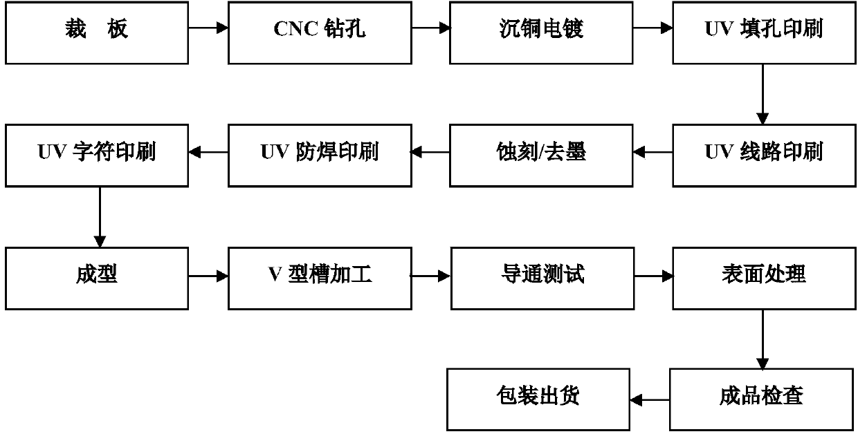
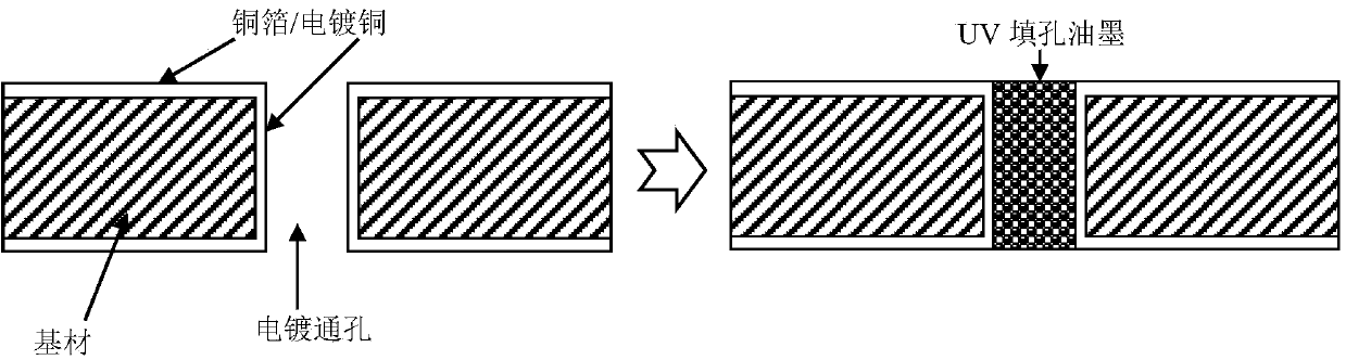
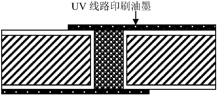
[0038] Such as figure 1 , figure 2 , image 3 , Figure 4 , Figure 5 , Figure 6 As shown, a UV printing process for manufacturing double-sided circuit boards with copper plated via holes includes cutting board—CNC drilling—copper plating—UV hole filling printing—UV circuit printing—etching / ink removal—UV Solder mask printing—UV character printing—forming—V-groove processing—conduction test—surface treatment—finished product inspection—packaging and shipping, the specific process is as follows:

[0039] (1) Cutting board: Cut the large-area copper-clad laminate provided by the manufacturer into the working size required for production;

[0040] (2) CNC drilling: Drill through holes on the cut copper-clad laminates, which are used to connect the plug-in holes of copper plating and welding parts on both sides of the circuit;

[0041] (3) Copper sinking electroplating: copper sinking electroplating treatment for via holes used for line connection;

[0042] (4) UV hole-fi...


PUM


Abstract

The invention provides a process for manufacturing electroless copper electroplating via hole type double-sided circuit board through the UV printing method. The process comprises the following processes: cutting a plate; drilling a hole by a CNC (Computerized Numerical Control) manner; performing electroless copper electroplating; filling the hole and printing through UV; printing circuit through UV; etching/ erasing ink; performing solder masking printing through UV; printing characters through UV; moulding; processing a V-shaped groove; conducting to test; processing the surface; examining a finished product; packaging and delivering. According to the technical scheme, the process has the advantages that the material cost is small, the processing can be quickly performed, the process is simple, less defective products are produced, the processing efficiency is high, and automatic liner mass production applies.

Description

technical field [0001] The invention relates to the technical field of printed circuit boards, in particular to a process for manufacturing double-sided circuit boards with sinking copper electroplating via holes by a UV printing method. Background technique [0002] As we all know, printed circuit boards (PCBs) are widely used as the basic material of the electronics industry. As small as electronic watches, calculators, personal computers, as large as computers, communication equipment, medical equipment, and aerospace or military equipment, as long as there are electronic components such as integrated circuits, PCBs are used for electrical interconnection between them. [0003] Existing double-sided circuit boards use double-sided copper-clad laminates on the copper foil layer for parallel exposure and development to make circuits. The process includes cutting boards—CNC drilling—copper plating—dry film. Development—etching. Ink removal—solder resist coating. Prebaking—e...

Claims


Application Information

Patent Timeline
Patent Type & Authority Applications(China)
IPC IPC(8): H05K3/00H05K3/42
Inventor 骆文林守伟李声红
Owner MISSION FE CO LTD
Why Eureka
Try Eureka