Liquid crystal display panel and manufacturing method thereof

A technology for liquid crystal display panels and manufacturing methods, applied in nonlinear optics, instruments, optics, etc., which can solve the problems of ITO electrodes not being able to conduct normally, ITO not being able to conduct, and screens not being displayed, etc.

Active Publication Date: 2014-12-17
NANJING CEC PANDA LCD TECH
View PDF7 Cites 17 Cited by
  • Summary
  • Abstract
  • Description
  • Claims
  • Application Information

AI Technical Summary

Problems solved by technology

[0012] Due to the strong fluidity of the inkjet alignment fluid, if not used figure 1 Retaining walls or gutters as shown, such as Figure 5 It is a schematic diagram of the alignment liquid flowing to cover the contact hole. The alignment liquid can easily cover the ITO 103 at the position of the contact hole 200. The alignment liquid is made of insulating material, which will c...

Method used


Image

  • Liquid crystal display panel and manufacturing method thereof
  • Liquid crystal display panel and manufacturing method thereof
  • Liquid crystal display panel and manufacturing method thereof

Examples


Embodiment Construction

[0049] In order to make the technical problems, technical solutions, and advantages to be solved by the embodiments of the present invention clearer, a detailed description will be given below with reference to the drawings and specific embodiments.

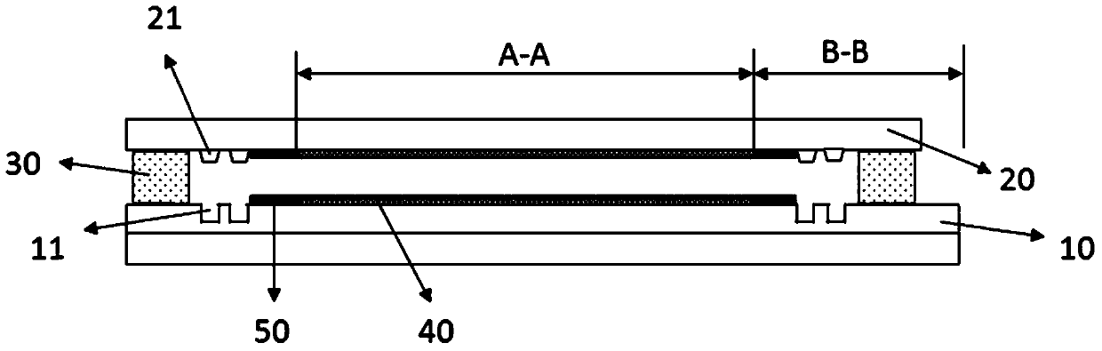
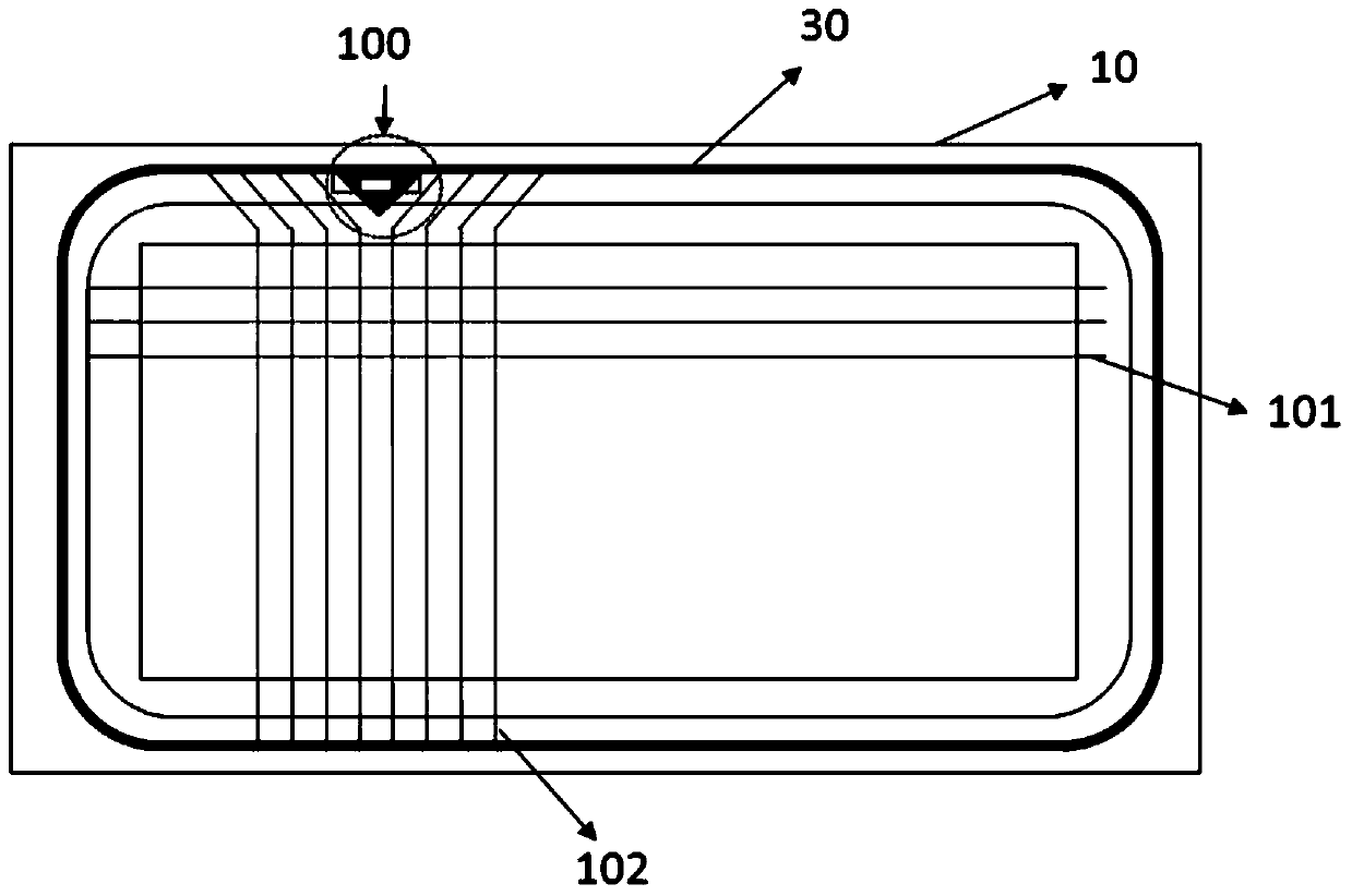
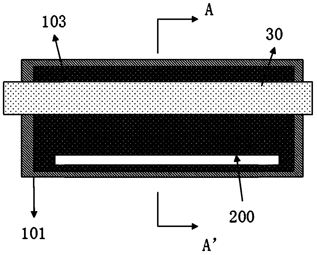
[0050] The present invention is based on the improvement where the existing alignment film flows under the sealant area, which causes the color film substrate and the ITO electrode on the array substrate to fail to conduct normally. The present invention uses the contact position of the array substrate and the color film substrate to specifically At the position of the sealant matching the array substrate and the color filter substrate, a semiconductor layer is provided under the ITO of the array substrate, and a color layer is provided under the black matrix layer of the corresponding color filter substrate, so that the opposite ITO forms an island pattern. It is an amorphous silicon, polysilicon or metal oxide layer with a thicknes...


PUM

PropertyMeasurementUnit
Thicknessaaaaaaaaaa

Abstract

The invention provides a liquid crystal display panel and a manufacturing method thereof. The liquid crystal display panel comprises an array substrate and a color film substrate which are oppositely arranged, wherein the array substrate and the color film substrate are adhered together through a sealant on the periphery; in an area corresponding to the sealant, a semiconductor layer is arranged below an ITO (Indium Tin Oxide) layer of the array substrate; a color layer is arranged in a black matrix layer of the color film substrate corresponding to the semiconductor layer. The semiconductor layer is arranged below the ITO on the array side of the peripheral area (contact position of the sealant), the color layer is arranged below BM on the side corresponding to the color film, and thus an island-shaped pattern is formed on the ITO, the thickness of an ordinary semiconductor layer is 2000 to 3000 Angstroms, the thickness of the color layer is 1.5 to 2 microns, and the increased height can effectively prevent PI from flowing to the upper part of the ITO.

Description

Technical field [0001] The present invention relates to the field of liquid crystal display technology, and in particular to a method for manufacturing a narrow frame liquid crystal display panel. Background technique [0002] Displays are indispensable in people’s daily lives. The types of displays include CRT (Cathode Ray Tube), LED (Light Emitting Diode), TFT-LCD (Thin Film Transistor-Liquid Crystal Display), and thin film transistor liquid crystal display. Display), PDP (Plasma Display Panel, Plasma), etc. At present, the vast majority of displays on the market are of TFT-LCD type. [0003] The TFT-LCD display is mainly composed of a color filter substrate and an array substrate that are arranged oppositely. The array substrate is subjected to an array process to form a circuit matrix (scanning line, data line, etc.) on the substrate, and the color film substrate is formed on the substrate through a color filter process. A black matrix and a red, green, and blue color film are...

Claims


Application Information

Patent Timeline
IPC IPC(8): G02F1/1362G02F1/1333
Inventor 王海宏焦峰
Owner NANJING CEC PANDA LCD TECH
Why Eureka
Try Eureka