Method for manufacturing semiconductor device

A semiconductor and device technology, applied in the field of manufacturing semiconductor devices, can solve the problems of poor adhesion between copper and the interlayer dielectric layer, increase the resistance value of the line resistance, affect the electrical performance of the interconnect structure, etc., to improve reliability and good quality. rate effect

Inactive Publication Date: 2014-12-24
SEMICON MFG INT (SHANGHAI) CORP
View PDF3 Cites 0 Cited by
  • Summary
  • Abstract
  • Description
  • Claims
  • Application Information

AI Technical Summary

Problems solved by technology

[0003] In the current copper interconnection process, copper as the wiring material has several serious disadvantages: it can quickly enter the adjacent interlayer dielectric region, which can lead to the formation of a conduction path between the two interconnect lines, resulting in Short circuit; at the same time, the adhesion between copper and the interlayer dielectric layer is also poor, and peeling is easy to occur
According to the prior art, a large number of silicon atoms are provided in the process of forming the CuSiN metal capping layer. In semiconductor devices, silicon atoms can make the device have a long electromigration lifetime, but, as figure 2 As shown, when more silicon atoms are provided to the semiconductor device during the process of forming the CuSiN metal capping layer, the excess silicon atoms will diffuse into the metal copper wiring, which will increase the resistance of the line resistance and affect the electrical properties of the interconnection structure. performance

Method used


Image

  • Method for manufacturing semiconductor device
  • Method for manufacturing semiconductor device
  • Method for manufacturing semiconductor device

Examples


Embodiment Construction

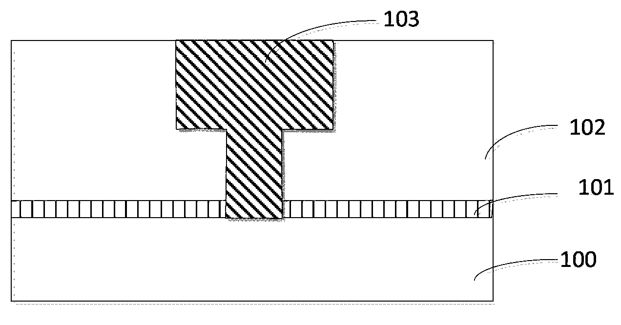
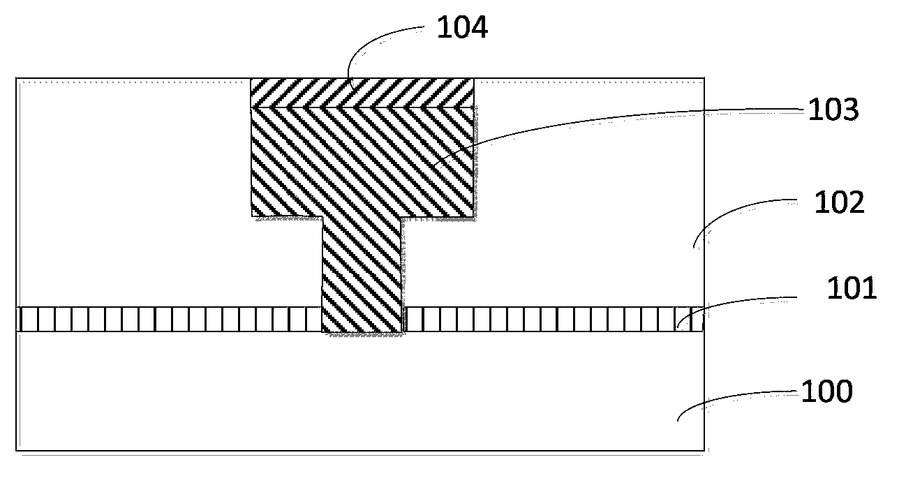
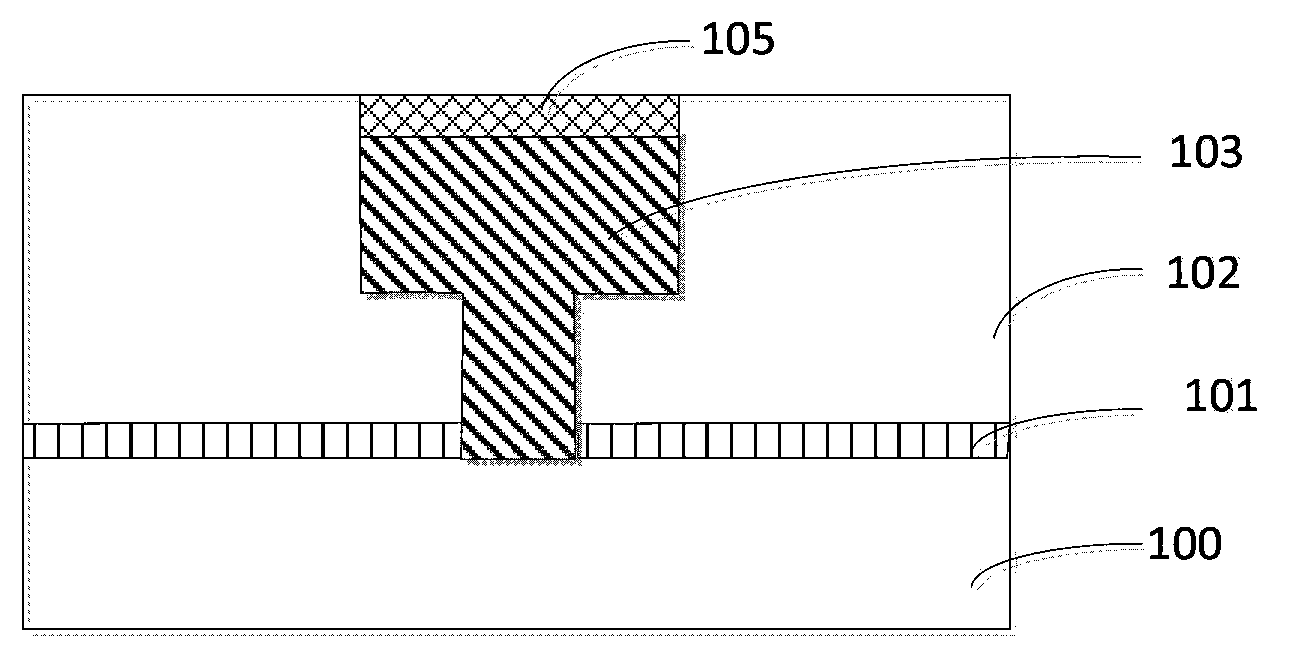
[0027] In the following description, numerous specific details are given in order to provide a more thorough understanding of the present invention. It will be apparent, however, to one skilled in the art that the present invention may be practiced without one or more of these details. In other examples, some technical features known in the art are not described in order to avoid confusion with the present invention.

[0028] In order to thoroughly understand the present invention, detailed steps will be proposed in the following description, so as to illustrate that the present invention proposes a method of using hexamethyldisilazane to treat the metal copper layer to form a metal covering layer, in order to balance the electrical The relationship between migration lifetime and wire resistance. Apparently, the preferred embodiments of the present invention are described in detail as follows, however, the present invention may also have other implementations apart from these...


PUM

PropertyMeasurementUnit
thicknessaaaaaaaaaa

Abstract

The invention discloses a method for manufacturing a semiconductor device. The method includes the following steps that a semiconductor substrate is provided; a low k interlayer dielectric layer and a metal interconnection structure located in the low k interlayer dielectric layer are formed on the semiconductor substrate; hexamethyldisilane is used for processing the exposed top face of the metal interconnection structure, so that a metal covering layer is formed; an electric dielectric covering layer is formed on the low k interlayer dielectric layer and the metal covering layer. According to the manufacturing technology, the hexamethyldisilane is used for processing a metal copper layer, so that the metal covering layer is formed, better adhesiveness, low wire resistance and the good electromigration performance are provided for the device, and the reliability and the yield of the device are improved.

Description

technical field [0001] The invention relates to a semiconductor manufacturing process, in particular to a method for manufacturing a semiconductor device. Background technique [0002] As semiconductor manufacturing technology becomes more and more sophisticated, integrated circuits are also undergoing major changes. The number of components integrated on the same chip has increased from the initial dozens or hundreds to the current millions. In order to meet the requirements of complexity and circuit density, the manufacturing process of semiconductor integrated circuit chips uses batch processing technology to form various types of complex devices on the substrate and interconnect them to have complete electronic functions. A low-k interlayer dielectric layer is used as a dielectric material to isolate each metal interconnection between the wires, and the interconnection structure is used to provide wiring between the device on the IC chip and the entire package. In this ...

Claims


Application Information

Patent Timeline
Patent Type & Authority Applications(China)
IPC IPC(8): H01L21/768
CPCH01L21/76856H01L2221/1084
Inventor 邓浩
Owner SEMICON MFG INT (SHANGHAI) CORP
Why Eureka
Try Eureka