Double-graphene-layer tunneling field effect transistor and manufacturing method thereof

A double-layer graphene and tunneling field effect technology, applied in the field of nanoelectronics, can solve the problems that limit the wide application of TFET, low tunneling probability, etc., and achieve the effect of small off-state current and simple preparation process

Active Publication Date: 2014-12-24
PEKING UNIV
View PDF2 Cites 14 Cited by
  • Summary
  • Abstract
  • Description
  • Claims
  • Application Information

AI Technical Summary

Problems solved by technology

However, the on-state current of TFET is limited by the low tunneling proba

Method used


Image

  • Double-graphene-layer tunneling field effect transistor and manufacturing method thereof
  • Double-graphene-layer tunneling field effect transistor and manufacturing method thereof
  • Double-graphene-layer tunneling field effect transistor and manufacturing method thereof

Examples


Embodiment Construction

[0038] The present invention will be further described below by example. It should be noted that the purpose of the disclosed embodiments is to help further understand the present invention, but those skilled in the art can understand that various replacements and modifications are possible without departing from the spirit and scope of the present invention and the appended claims of. Therefore, the present invention should not be limited to the content disclosed in the embodiments, and the protection scope of the present invention is subject to the scope defined in the claims.

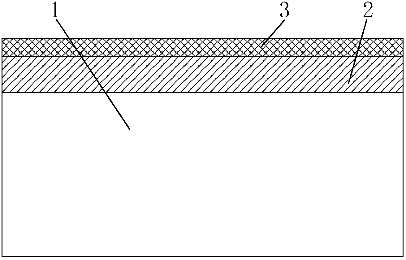
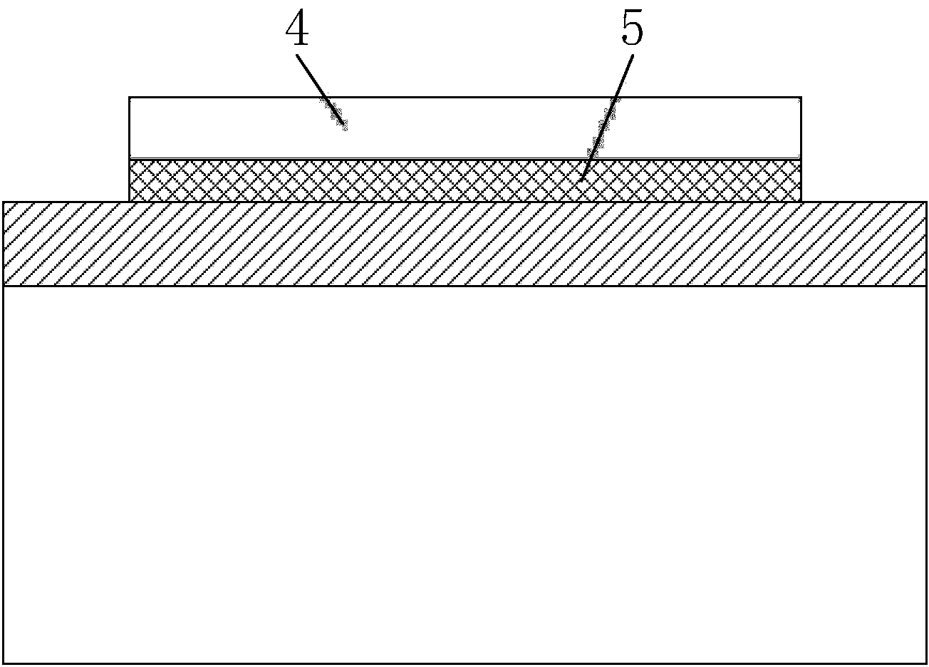
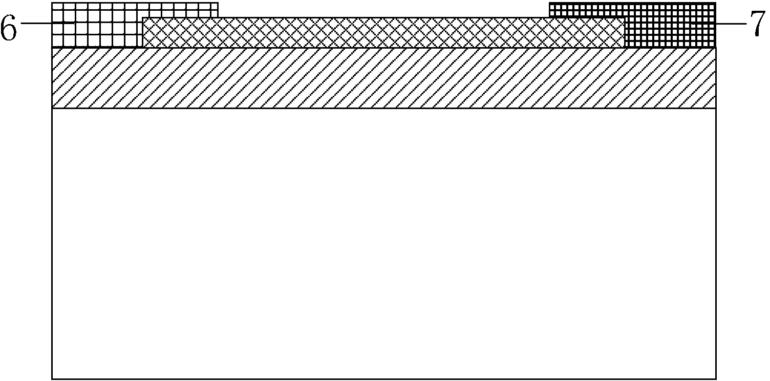
[0039] A specific example of the preparation method of the present invention includes Figure 1 to Figure 5 Process steps shown:

[0040] 1) A low-resistance silicon wafer with (100) crystal orientation is used as the bottom gate electrode 1, and a layer of bottom gate dielectric layer 2 is thermally oxidized on its surface, and the bottom gate dielectric layer is SiO 2 , with a thickness of 90nm;...


PUM


Abstract

The invention provides a double-graphene-layer tunneling field effect transistor. A bottom gate dielectric layer is located on a bottom gate electrode. A double-graphene-layer active area is located on the bottom gate dielectric layer. A metal source electrode and a metal drain electrode are located at the two ends of the double-graphene-layer active area respectively and respectively cover a part of the double-graphene-layer active area. The metal source electrode and the metal drain electrode are made of different materials. For an n-type device, the work function of the metal source electrode is larger, the graphene in contact with the metal source electrode is in p-type doping, the work function of the metal drain electrode is small, and the graphene in contact with the metal drain electrode is in n-type doping. The electrodes of a p-type device are opposite to those of the n-type devices. The metal source electrode, the metal drain electrode and the graphene between the metal source electrode and the metal drain electrode are covered with a top gate dielectric layer. A top gate electrode is located on the top gate dielectric layer and overlaps the metal source electrode and the metal drain electrode. The manufacturing technology of the double-graphene-layer tunneling field effect transistor is simple. Compared with a traditional double-graphene-layer field effect transistor, the metal source electrode and the metal drain electrode of the double-graphene-layer tunneling field effect transistor are completed independently.

Description

technical field [0001] The invention belongs to the technical field of nanoelectronics, and in particular relates to a double-layer graphene tunneling field-effect transistor based on metal contact doping and a preparation method thereof. Background technique [0002] As the feature size of conventional MOSFETs decreases, the operating and threshold voltages of the devices gradually decrease. Since the subthreshold slope of the MOSFET is limited by the thermal potential, there is a theoretical limit of 60mV / dec, which cannot be reduced with the reduction of the device size, so the leakage current of the device increases with the reduction of the operating voltage. In addition, the short-channel effect of small-sized devices is more obvious, and the leakage-induced barrier reduction and source-drain band-band tunneling will further increase leakage current and power consumption. At present, the problem of power consumption has become a key concern in the design of small-scal...

Claims


Application Information

Patent Timeline
IPC IPC(8): H01L29/78H01L21/336H01L29/41H01L29/43
CPCH01L29/41725H01L29/43H01L29/66356H01L29/7391
Inventor 黄如王佳鑫黄芊芊吴春蕾朱昊赵阳
Owner PEKING UNIV
Why Eureka
Try Eureka