

Organic electroluminescent display device, manufacturing method thereof and display unit
An electroluminescence display and display device technology, applied in organic semiconductor devices, materials of organic semiconductor devices, electric solid devices, etc., can solve the problem of low luminous efficiency of OLED devices, low hole transport efficiency, and holes that are not easy to pass through. and other problems to achieve the effect of improving the luminous performance, improving the degree of balance, and increasing the number of
- Summary
- Abstract
- Description
- Claims
- Application Information
AI Technical Summary
Problems solved by technology
Method used
Image

Examples
Embodiment Construction
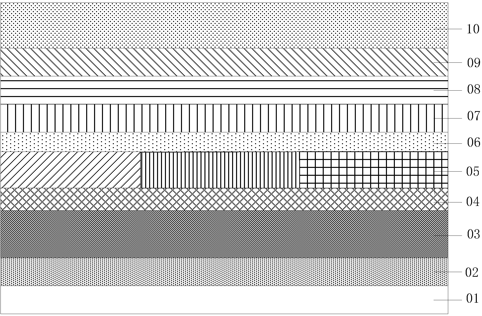
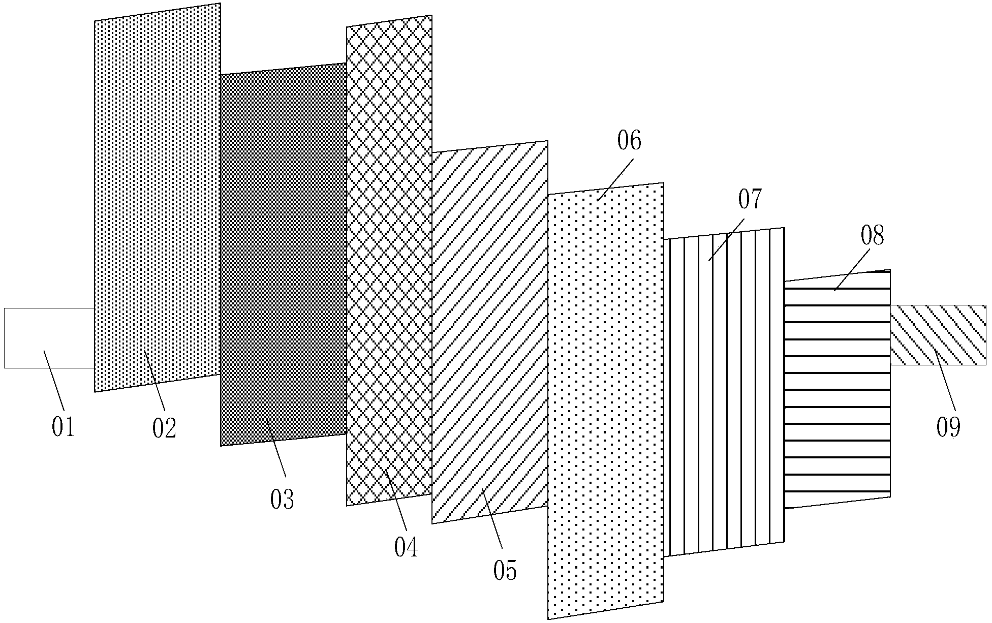
[0027] The specific implementation manners of the organic electroluminescent display device provided by the embodiments of the present invention, its manufacturing method and the display device will be described in detail below with reference to the accompanying drawings.
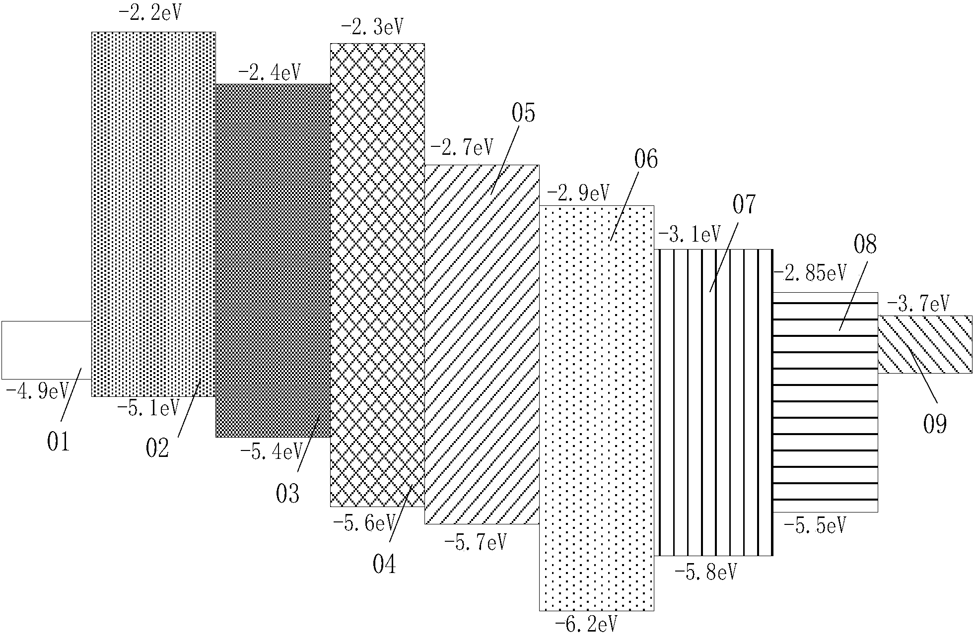
[0028] Wherein, the thickness and shape of each film layer in the drawings do not reflect the real scale of the organic electroluminescent display device, and the purpose is only to illustrate the content of the present invention.
[0029] An embodiment of the present invention provides an organic electroluminescent display device, such as Figure 4a As shown, it includes: a base substrate 20, a hole injection layer 02, a hole transport layer 03 and an electron blocking layer 04 sequentially arranged on the base substrate 20; wherein, the material of the hole transport layer 03 is a P-type doped Miscellaneous materials.
[0030] Since the material of the hole transport layer 03 in the above-mentioned organ...
PUM
 Abstract
Description
Claims
Application Information