
Mask unit and substrate processing device

A substrate processing device and substrate technology, which is applied in the direction of exposure devices, electrical components, optics, etc. of photolithography, and can solve the problems such as the inability to obtain projection image adjustment functions, etc.

Active Publication Date: 2016-04-20
NIKON CORP
View PDF9 Cites 0 Cited by
  • Summary
  • Abstract
  • Description
  • Claims
  • Application Information

AI Technical Summary

Problems solved by technology

[0013] In addition, the proximity exposure method in which the rotating drum on which the sheet (substrate) is wound is brought close to the cylindrical mask cannot achieve the adjustment function of the projected image like the projection exposure method.
Therefore, it is difficult to easily fine-tune the relative positional relationship between the mask pattern and the sheet (substrate) (especially magnification correction)

Method used


Image

  • Mask unit and substrate processing device
  • Mask unit and substrate processing device
  • Mask unit and substrate processing device

Examples


Embodiment Construction

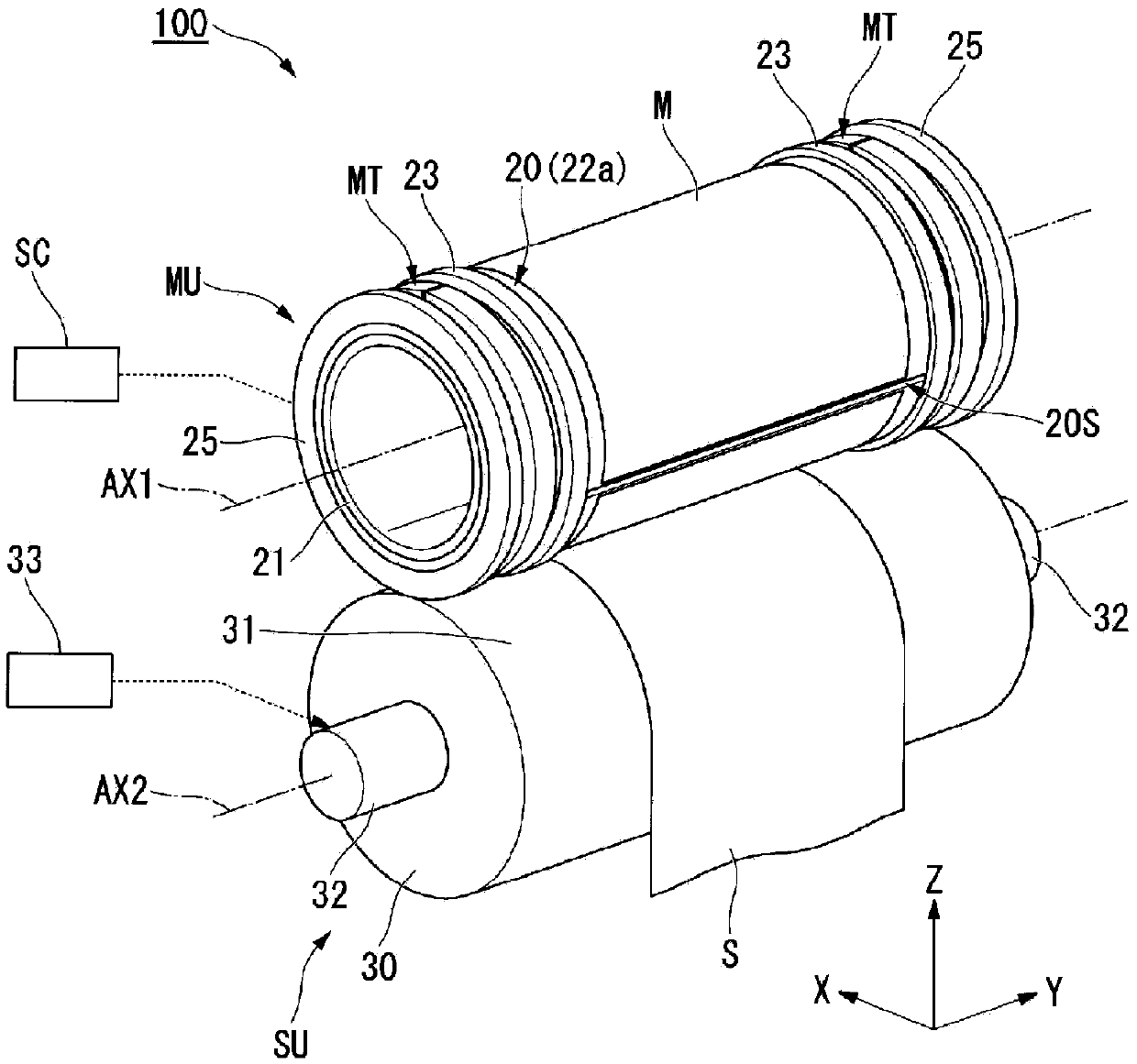
[0029] Below, refer to Figure 1 to Figure 7 Embodiments of the mask unit and the substrate processing apparatus of the present invention will be described.

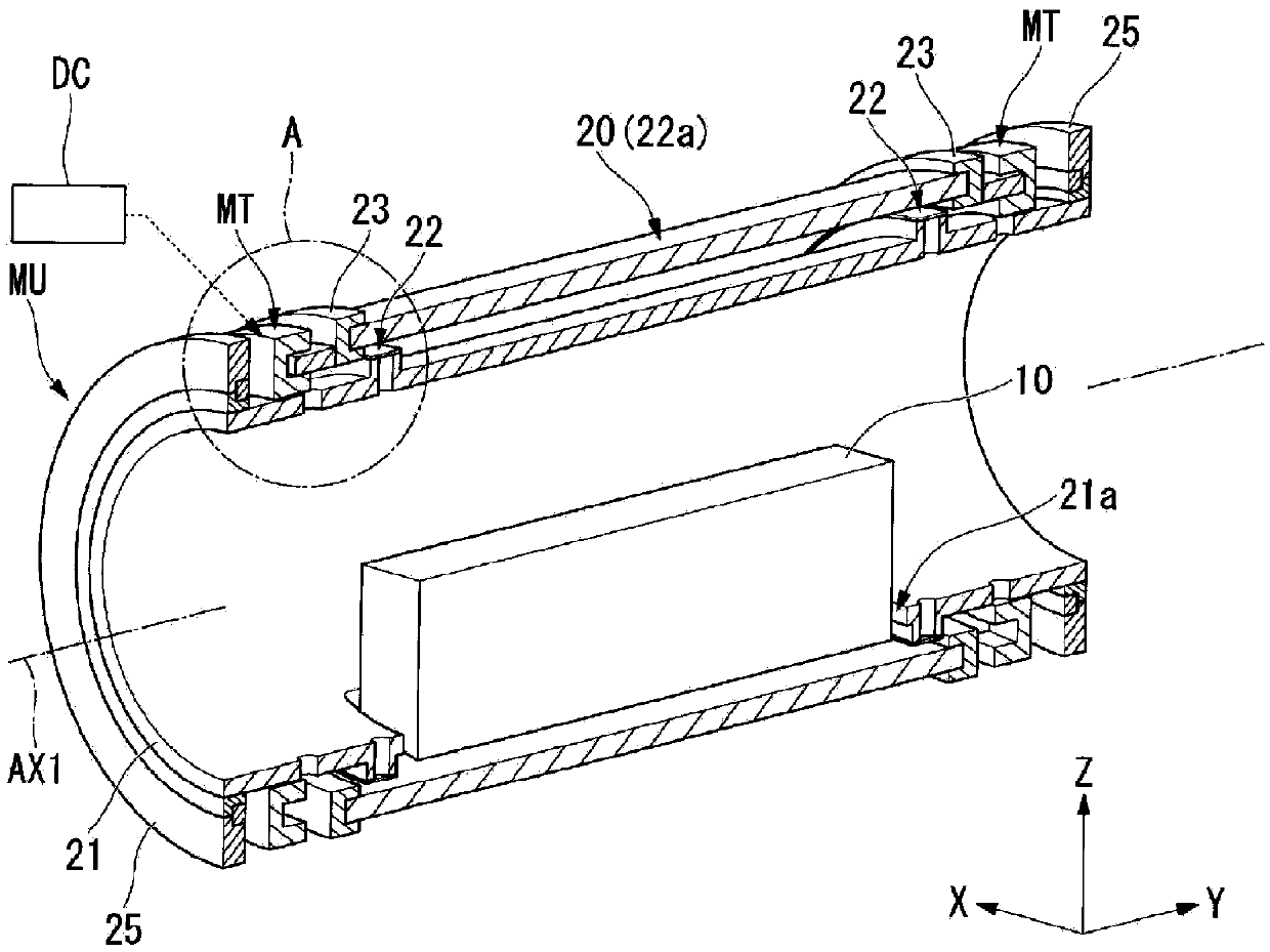
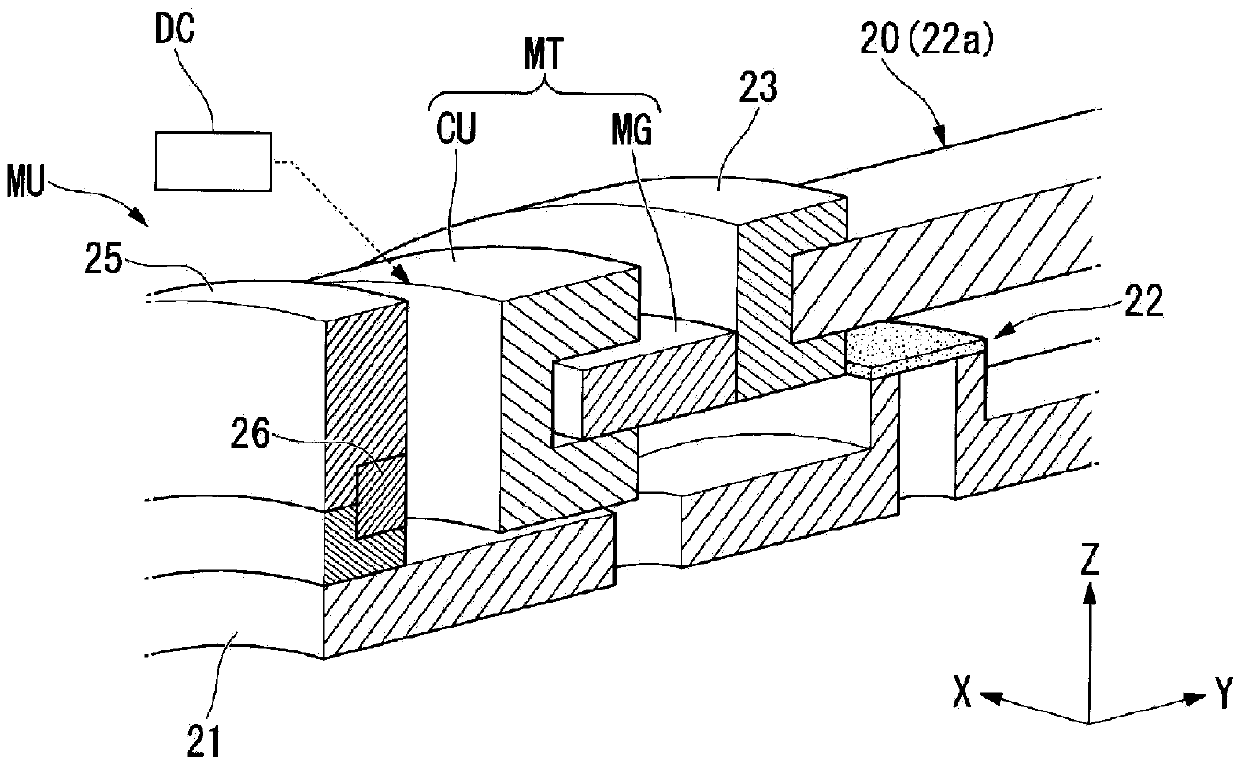
[0030] figure 1 It is a schematic external perspective view of a substrate processing apparatus 100 including a rotatable cylindrical mask unit MU and a sheet (substrate) S holding unit SU. figure 2 It is cut with the plane containing its axis of rotation AX1 figure 1 Cross-sectional view of the cylindrical mask unit MU in . image 3 is true figure 2 A magnified view of part A.

[0031] The substrate processing apparatus 100 is an apparatus for exposing a strip-shaped substrate (for example, a strip-shaped film member) S to a pattern of a flexible sheet-shaped mask M. The substrate processing apparatus 100 is mainly composed of an illumination unit 10 ( figure 1 not shown in the figure, refer to figure 2 ), a mask unit MU, a substrate holding unit SU, and a control unit (not shown).

[0032] In this embodiment...


PUM


Abstract

A mask unit comprises: a mask holding unit (20) which holds a mask pattern on a cylindrical surface with a prescribed radius centered on a first axial line (AX1) and is rotatable around the first axial line; a support unit (22) for supporting the mask holding unit in a contactless or low friction state so that the mask holding unit is able to rotate around and move in the direction of the first axial line; and a pair of driving units (MT) which is provided on both sides in the first axial line direction of the mask holding unit and drives the mask holding unit by propelling the mask holding unit to rotate around the first axial line.

Description

technical field [0001] The present invention relates to a mask unit and a substrate processing device. [0002] This application claims priority based on Japanese Patent Application No. 2012-095894 for which it applied on April 19, 2012, and uses the content here. Background technique [0003] In a large-screen display device such as a liquid crystal display device, first, a transparent electrode such as ITO (Indium Tin Oxide) and a semiconductor such as Si are deposited on a flat glass substrate, and then a metal material is deposited, and a photoresist is applied and transferred. circuit pattern. Thereafter, after developing the photoresist, a circuit pattern and the like are formed by etching. However, as the size of the glass substrate increases with the increase in the screen size of the display element, it becomes difficult to transport the substrate. Therefore, it has been proposed to form a display element on a flexible substrate (for example, a film member such a...

Claims


Application Information

Patent Timeline
Patent Type & Authority Patents(China)
IPC IPC(8): G03F7/24G03F7/20H01L21/027H01L21/683
CPCG03F7/24
Inventor 铃木智也
Owner NIKON CORP
Learn More