Photomask blank, photomask and fabrication method thereof

A technology for photomasks and light-shielding films, applied in the field of photomasks, can solve problems such as hindering defect inspection, high film reflectivity, and the inability of photomask blank structures to satisfy fine photomask patterns satisfactorily. Increase dry etching rate, ensure etching resistance, and reduce thickness

Active Publication Date: 2007-01-24
SHIN ETSU CHEM IND CO LTD +1
View PDF12 Cites 25 Cited by
  • Summary
  • Abstract
  • Description
  • Claims
  • Application Information

AI Technical Summary

Problems solved by technology

However, if SiO 2 film as an etch mask, there will be SiO 2 Problems with excessively high film reflectivity, which hinders defect inspection
[0017] As described above, conventional photomask blank structures cannot satisfactorily meet the demand for forming fine photomask patterns on light shielding films with high precision.

Method used


Image

  • Photomask blank, photomask and fabrication method thereof
  • Photomask blank, photomask and fabrication method thereof
  • Photomask blank, photomask and fabrication method thereof

Examples


Embodiment 1

[0065] (Example 1: Light-shielding film of photomask blank according to the present invention)

[0066] In order to reduce the thickness of the photoresist used as a mask for forming a photomask pattern, it is necessary to reduce damage to the light-shielding film during etching of the light-shielding film in which the photoresist mask is patterned. To this end, it is necessary to reduce the time required to etch the light-shielding film by reducing the physical thickness of the light-shielding film to be patterned and / or by increasing the etching rate of the light-shielding film.

[0067] The inventor’s investigation and research prove that increasing the etching rate of the light-shielding film can be achieved by reducing the metal percentage content in the light-shielding film. This means that high-rate etching can be achieved by designing the commonly used chromium-based shading film to reduce the chromium content (percentage content) in the shading film.

[0068] For example,...

Embodiment 2

[0120] (Example 2: Basic structure of photomask blank)

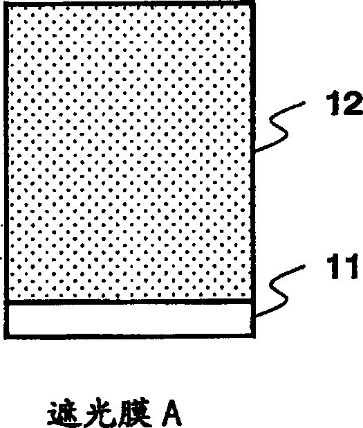
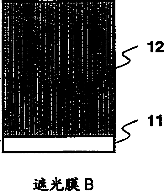
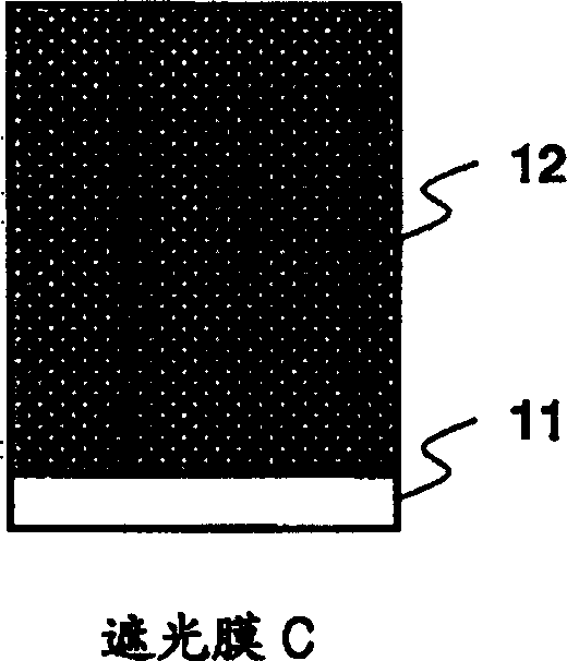
[0121] Figure 9A It is a schematic cross-sectional view for explaining an exemplary structure of a photomask blank according to the present invention, in which a light-shielding film 12 is formed on one principal plane of a transparent substrate 11 made of quartz or the like and used as a photomask substrate on. The light-shielding film 12 has a layered structure as described above with respect to Example 1, which serves not only as a "light-shielding film" but also as an anti-reflection film. The film with this composition is used because it has excellent dry etching properties, electrical conductivity and chemical resistance.

[0122] In the case where the photomask blank according to the present invention is designed to be used for making an ArF exposure mask, the thickness and composition of the light-shielding film 12 are selected so that the optical density OD of the light-shielding film 12 for light with a wavelengt...

Embodiment 3

[0132] (Embodiment 3: Photomask blank and the first embodiment of patterning process)

[0133] Picture 10 Showing an exemplary arrangement of a film deposition apparatus (sputtering apparatus) used to make a photomask blank according to the present invention, Figure 11A to 11D It is a view for explaining an exemplary process of patterning the photomask blank.

[0134] in Picture 10 Here, reference numeral 11 denotes a transparent substrate, which is a 6-inch rectangular quartz substrate. Generally, the surface and end faces of the quartz substrate are finely polished. Reference numeral 101 represents a cavity, reference numeral 102a represents a first target (target), reference numeral 102b represents a second target, reference numeral 103 represents a sputtering gas inlet, reference numeral 104 represents a gas outlet, reference numeral 105 represents a substrate turntable, and reference numerals 106a and 106b respectively represent the first target. One and the second target...


PUM

PropertyMeasurementUnit
thicknessaaaaaaaaaa
thicknessaaaaaaaaaa
thicknessaaaaaaaaaa

Abstract

PROBLEM TO BE SOLVED: To provide a halftone type phase shift mask on which a fine photomask pattern is formed with high accuracy, and to provide a mask blank for producing the above mask. ŽSOLUTION: A semitransparent film 15 having a predetermined phase shift and transmittance to exposure light and a light shielding film 12 placed on the semitransparent film 15 are disposed on one principal face of a transparent substrate 11 such as quartz as a photomask substrate. The light shielding film 12 is surely a so-called "light shielding film" but it can also act as an antireflection film. The semitransparent film 15 is a halftone phase shift layer comprising a halftone material containing both of silicon (Si) and molybdenum (Mo) as an absorbent material. In order to use the halftone phase shift mask blank for producing a mask for ArF exposure, the film thickness and composition of the light shielding film 12 are selected to obtain the optical density OD of the film in the range of 1.2 to 2.3 with respect to light at 193 or 248 nm wavelength. Ž

Description

Technical field [0001] The present invention relates to photomasks, photomask blanks used as raw materials for photomasks, and methods for making them. Background technique [0002] In recent years, the increase in the packaging density of large integrated circuits requires the miniaturization of circuit patterns. In order to meet the demand for such miniaturization, advanced semiconductor micromachining technology has become extremely important. For example, the increase in the packaging density of large integrated circuits essentially requires a technique for thinning the wires of wiring patterns in the circuit, or a technique for miniaturizing contact hole patterns used for interweaving wiring units. The trend of miniaturization of the circuit patterns of such large integrated circuits is accelerating because it is the most effective way to increase the operation speed and reduce energy consumption. [0003] Most of these advanced micromachining technologies are based on photo...

Claims


Application Information

Patent Timeline
Patent Type & Authority Applications(China)
IPC IPC(8): G03F1/14G03F7/16C23C14/06G03F1/32G03F1/58G03F1/68H01L21/027
Inventor 吉川博树洼田宽木名濑良纪冈崎智丸山保原口崇岩片政秀福岛祐一佐贺匡
Owner SHIN ETSU CHEM IND CO LTD
Why Eureka
Try Eureka