Electro-optical device, method of manufacturing the same, and electronic apparatus using electro-optical device

a technology of electro-optical devices and optical components, applied in the direction of picture reproducers, identification means, instruments using projection devices, etc., can solve the problems of difficult drawing gap materials on boundary lines, change in characteristics of tft, and difficulty in obtaining sufficient aperture ratio, etc., to achieve uniform lens performance, improve image quality, and improve image quality

Inactive Publication Date: 2005-12-15
SEIKO EPSON CORP
View PDF11 Cites 23 Cited by
  • Summary
  • Abstract
  • Description
  • Claims
  • Application Information

AI Technical Summary

Benefits of technology

[0018] An advantage of the invention is that it provides to an electro-optical device that can uniformize the thickness of a microlens layer to realize uniform lens performance and that can sufficiently cope with demands for higher image quality, a method of manufacturing such an electro-optical device, and an electronic apparatus using such an electro-optical device.
[0019] According to a first aspect of the invention, an electro-optical device includes first and second substrates that face each other, and support bodies that are provided between both substrates so as to define a gap between both substrates. The first substrate is a lens glass substrate that has a plurality of concave portions and the second substrate is a cover glass substrate that faces the first substrate. A microlens layer is formed between both substrates and a thickness of the microlens layer is defined by the support bodies.
[0020] According to this configuration, the gap between the lens glass substrate and the cover glass substrate is defined by the support bodies. Therefore, the support bodies can be formed on the boundary of adjacent concave portions. As a result, the thickness of the microlens layer can be made uniform, resulting in uniform lens performance.
[0021] In the electro-optical device according to the first aspect of the invention, it is preferable that the support bodies are made of a curable material ejected from a liquid droplet ejection unit.
[0022] According to this configuration, the support bodies are made of the curable material ejected from the liquid droplet ejection unit. Therefore, the support bodies can be formed in narrow areas with high precision.
[0023] In the electro-optical device according to the first aspect of the invention, it is preferable that a gap material that defines a distance between both substrates is mixed in the supporting bodies.

Problems solved by technology

In such an active-matrix-type liquid crystal device, a high contrast ratio is easily obtained, but a TFT, a capacitive element, and the like need to be provided for each pixel, which results in a problem in that a sufficient aperture ratio is difficult to obtain.
Further, when intense light is irradiated onto a channel region or a drain terminal of the TFT, photocurrent is generated, which causes a change in characteristics of the TFT.
However, if the interval between the counter substrates is reduced, it is difficult to draw the gap material on the boundary lines between the counter substrates with the dispenser or the like.
Then, uniformity of the products is difficult to maintain.
Accordingly, such demands result in defective products.

Method used


Image

  • Electro-optical device, method of manufacturing the same, and electronic apparatus using electro-optical device
  • Electro-optical device, method of manufacturing the same, and electronic apparatus using electro-optical device
  • Electro-optical device, method of manufacturing the same, and electronic apparatus using electro-optical device

Examples


first embodiment

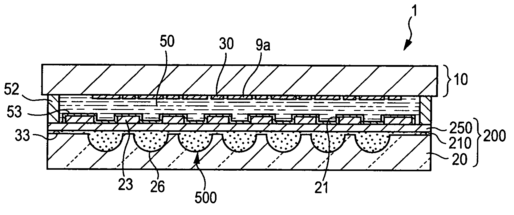
[0093] FIGS. 1 to 7 relate to the first embodiment of the invention. A substrate with a microlens array may be used for various optical apparatuses. In the present embodiment, for example, the substrate with the microlens array is applied to a counter substrate of a liquid crystal device serving as a light valve of a projection-type display device, which is an example of an electronic apparatus.

[0094]FIG. 1 is a cross-sectional view of a liquid crystal device. The overall configuration of a liquid crystal device, which is an example of an electro-optical device, will be described with reference to FIG. 1. Here, for example, a TFT active-matrix-type liquid crystal device having a built-in driving circuit will be described.

[0095] The liquid crystal device 1 of the present embodiment has a counter substrate 200 and an active matrix substrate 10 made of a quartz substrate, which are bonded to each other via a sealing material 52 with a space defining a predetermined gap. Liquid crysta...

first example

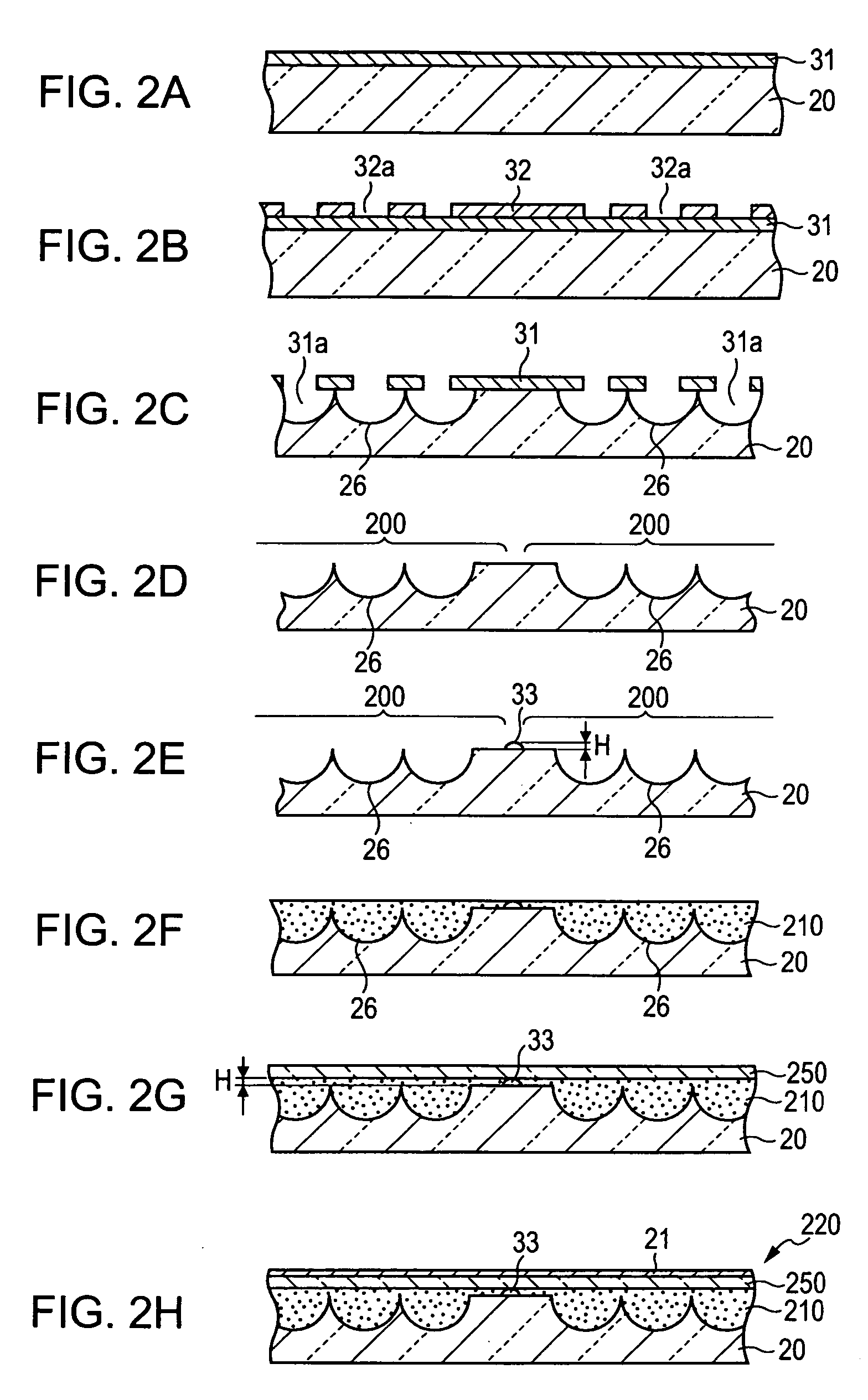
[0116] A first example of the unit that draws the support bodies 33 on the lens glass substrate 20 in the form of dots will be specifically described with reference to FIG. 4. FIG. 4 is an expanded cross-sectional view showing essential parts in a state where the support bodies are drawn, according to the present example.

[0117] In the present example, a curable material forming the support bodies 33 is ejected by a predetermined amount onto the surface of the lens glass substrate 20 from the liquid droplet ejection device main body 300. When the curable material is attached to the lens glass substrate 20, the support bodies 33, each having the height H, are formed by surface tension.

[0118] Here, the configuration of a liquid droplet ejection main body 300 will be simply described. The liquid droplet ejection main body 300 corresponds to a head of an inkjet printer and has a piezoelectric element 301 that constitutes an ultrasonic wave generating section. Electrodes (not shown) are...

second example

[0130] A second example of the unit that draws the support bodies 33 on the lens glass substrate 20 in the form of dots will be specifically described with reference to FIG. 5.

[0131] In the first example, the height H of each of the support bodies 33 is set by surface tension of the curable material. In the present example, a curable material, in which gap materials 34 are mixed, is ejected from the liquid droplet ejection device main body 300 by a predetermined amount and is drawn on the lens glass substrate 20 in the form of dots, thereby forming the support bodies 33.

[0132] In the liquid reservoir section 304 of the liquid droplet ejection device main body 300, the curable material, which is diluted by a solution, and the gap materials 34 are supplied. The gap materials 34 are made of glass fibers, glass beads, or the like and are spheres each having a particle size of from 5 to 20 μm. For actual use, the particle size is determined according to the height H of each of the supp...


PUM

PropertyMeasurementUnit
diameteraaaaaaaaaa
particle sizeaaaaaaaaaa
thicknessaaaaaaaaaa

Abstract

An electro-optical device includes first and second substrates that face each other, support bodies that are interposed between both substrates so as to define a gap between both substrates, and a microlens layer that is formed between both substrates. The first substrate is a lens glass substrate that has a plurality of concave portions and the second substrate is a cover glass substrate that faces the first substrate. A thickness of the microlens layer is defined by the support bodies.

Description

BACKGROUND OF THE INVENTION [0001] 1. Technical Field [0002] The present invention relates to an electro-optical device, in which a gap between a pair of substrates facing each other is defined by support bodies made of an adhesive ejected from a liquid droplet ejection device main body, to a method of manufacturing an electro-optical device, and to an electronic apparatus using such an electro-optical device. [0003] 2. Related Art [0004] A projection-type display device, such as a liquid crystal projector, or the like, has a configuration in which light irradiated from a light source is optically modulated by an electro-optical device serving as a light valve, and modulated light is projected to the front in a magnified scale. As a liquid crystal device that is an example of the electro-optical device, an active-matrix-type liquid crystal display is widely used in order to provide increased display quality. [0005] In the active-matrix-type liquid crystal device, pixels having pixel...

Claims


Application Information

Patent Timeline
Patent Type & Authority Applications(United States)
IPC IPC(8): G02F1/1335G02B3/00H01L21/00H01L51/52G09F9/00H01L33/00H04N9/31
CPCG02F1/133526H01L51/5275H04N9/3105H10K50/858G02F1/1335
Inventor SUZUKI, TOMIO
Owner SEIKO EPSON CORP
Why Eureka
Try Eureka