
Single Event Upset and Single Event Transient Immunity Latch

A single-event transient and anti-single-event technology, applied in the direction of pulse technology, electrical components, logic circuits, etc., can solve the problems of unable to shield combinational logic, unsuitable for high-reliability integrated circuit systems, soft errors, etc., and achieve power consumption And the effects of small area overhead, high reliability, and improved radiation resistance performance

Active Publication Date: 2017-05-31
HEFEI UNIV OF TECH
View PDF4 Cites 0 Cited by
  • Summary
  • Abstract
  • Description
  • Claims
  • Application Information

AI Technical Summary

Problems solved by technology

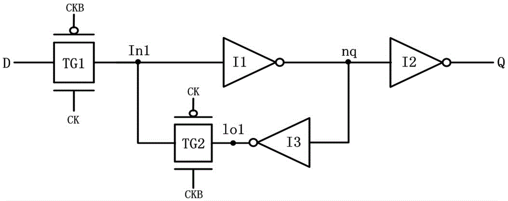
However, since many designs using the Radiation Hardened Design (RHBD) method inevitably have unprotected sensitive nodes, and the underlying components have not been redesigned using the Process Library Hardening (RHBP) method, such latches are bombarded by high-energy particles It will still cause soft errors, so it is not suitable for integrated circuit systems that strictly require high reliability
[0007] In addition, many designs using the above two design methods cannot shield SET from combinational logic

Method used


Image

  • Single Event Upset and Single Event Transient Immunity Latch
  • Single Event Upset and Single Event Transient Immunity Latch
  • Single Event Upset and Single Event Transient Immunity Latch

Examples


Embodiment Construction

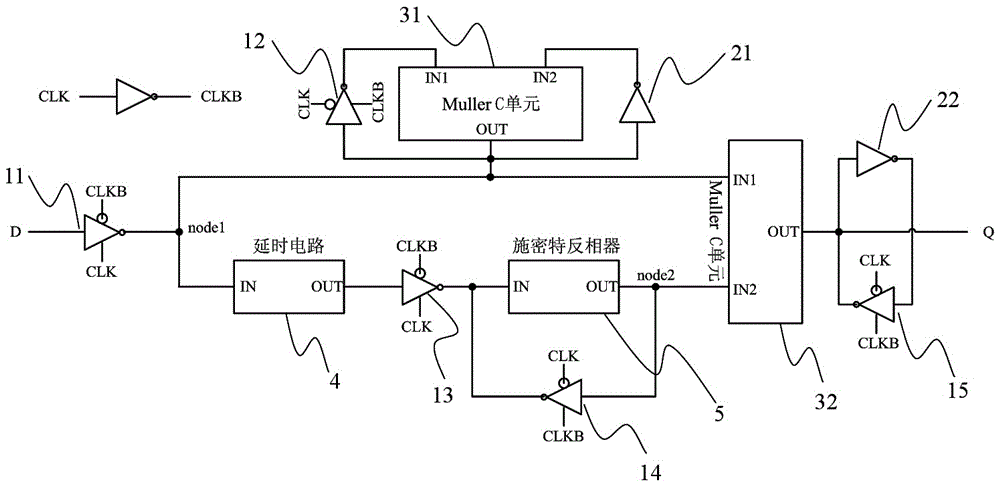
[0027] In order to make the purpose, technical solution and advantages of the present invention clearer, the present invention will be further described in detail below in conjunction with the accompanying drawings. The specific implementation cases described here are only used to illustrate the present invention, and are not intended to limit the present invention. figure 2 Shown is the schematic diagram of the latch circuit of the present invention, and its specific structure is as follows:

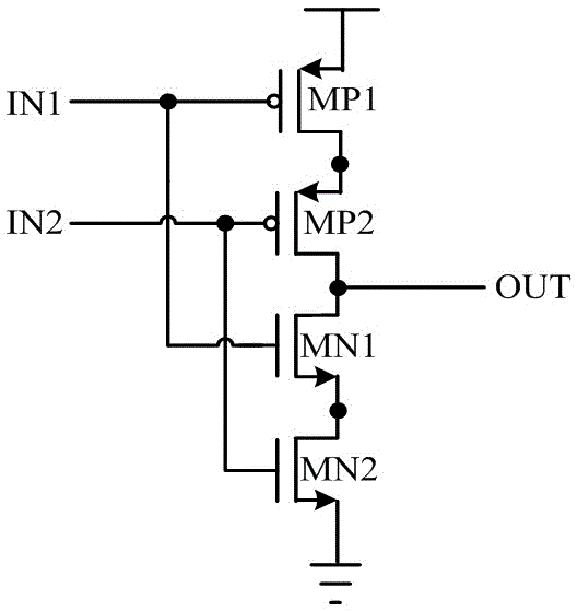
[0028] A latch resistant to single-event upsets and single-event transient pulses, comprising five clocked inverters, two conventional inverters, two Muller C cell circuits, a delay circuit4, and a Schmitt Inverter 5; the five clocked inverters are successively the first clocked inverter 11, the second clocked inverter 12, the third clocked inverter 13, and the fourth clocked inverter 14 and the fifth clocked inverter 15; two conventional inverters are the first conventional inverter ...


PUM


Abstract

The invention aims at the problems of poor SEU (Single Event Upset) resistance, poor SET (Single Event Transient) resistance, complicated structure and high cost of the existing integrated circuit, and provides a latch capable of resisting single event upset and single event transient pulse for implementing shielding of the SET from combinational logic and the SEU of data in the latch. The latch comprises five clock-controlled inverters, two regular inverters, two MullerC unit circuits, a Schmidt inverter and a delay circuit. The SEU and the SET are filtered by utilizing the MullerC unit circuits. The Schmidt inverter is used for increasing key charge of a sensitive node. The delay circuit is used for generating a signal in a delayed form. According to the latch capable of resisting single event upset and single event transient pulse, the influence of radiation on the circuit can be effectively eliminated, and the latch has the advantages of better anti-radiation performance, simple circuit structure and small area expenditure.

Description

technical field [0001] The invention relates to the technical field of semiconductor devices, and is especially applied in the field of anti-radiation integrated circuits, in particular to a latch anti-single-event reversal and single-event transient pulse. Background technique [0002] With the continuous advancement of science and technology and the rapid development of applications such as aerospace, aviation and nuclear energy, more and more electronic systems need to work in a radiation environment and are always facing the threat of radiation effects. Minority carriers are generated when energetic particles penetrate the silicon wafer, and if the minority carriers are neutralized by source / drain diffusion motions, this can lead to a change of state at such nodes. This phenomenon is called Single Event Transient (Single Event Transient, SET); if the transient fault is captured by the sampling element, a Single Event Upset (Single Event Upset, SEU) will occur and cause a...

Claims


Application Information

Patent Timeline
Patent Type & Authority Patents(China)
IPC IPC(8): H03K19/094
Inventor 黄正峰彭小飞鲁迎春梁华国易茂祥欧阳一鸣闫爱斌
Owner HEFEI UNIV OF TECH
Learn More