
Substrate-free LED device and manufacturing method thereof

A technology of LED devices and manufacturing methods, which is applied in the direction of semiconductor devices, electrical components, circuits, etc., can solve the problems of no improvement in heat dissipation of the packaging structure, reduction of packaging size, reduction of packaging cost and thickness, etc., so as to save costs and process steps, Effects of improved reliability and improved flexibility

Inactive Publication Date: 2015-01-28
杨晓丽
View PDF6 Cites 5 Cited by
  • Summary
  • Abstract
  • Description
  • Claims
  • Application Information

AI Technical Summary

Problems solved by technology

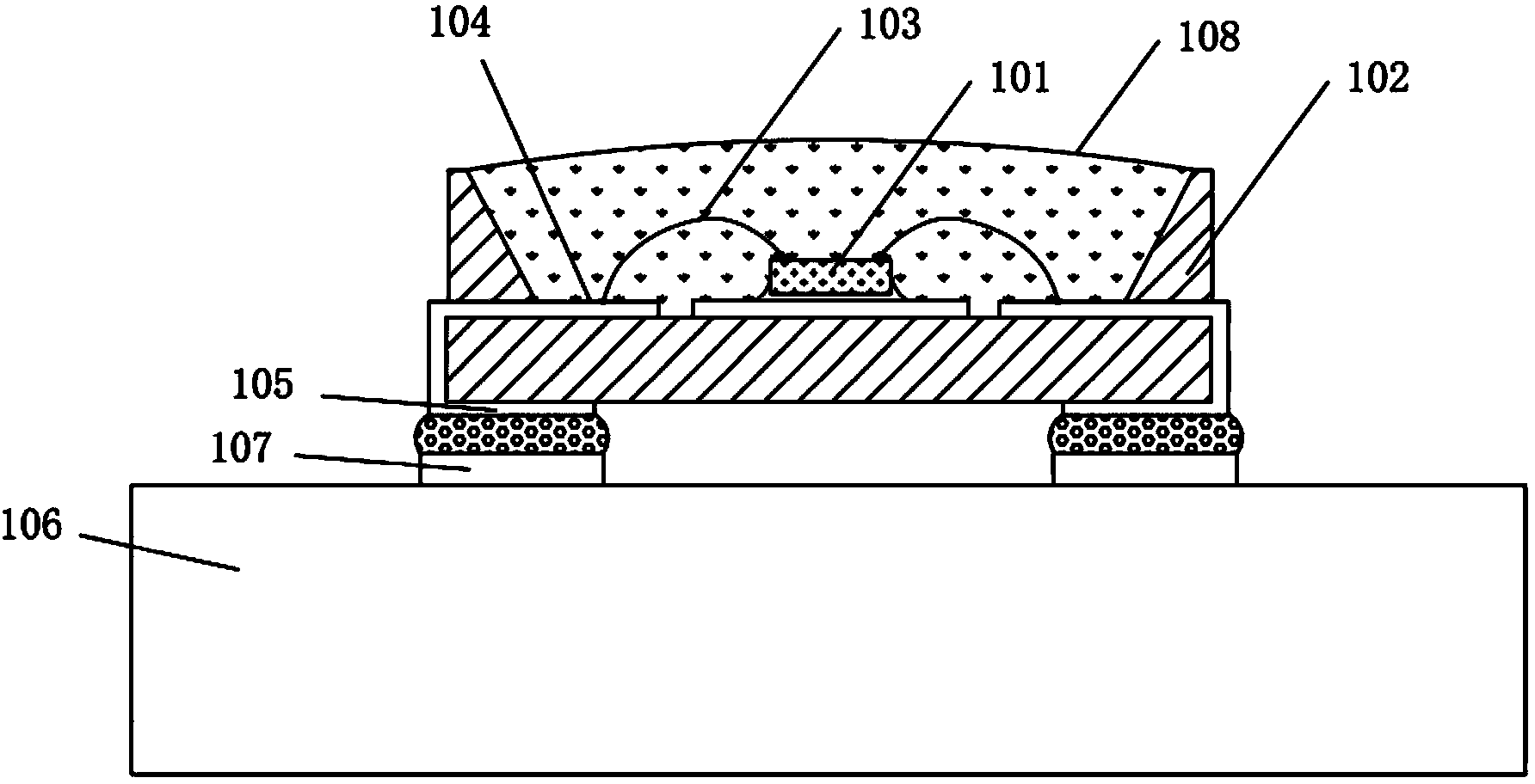
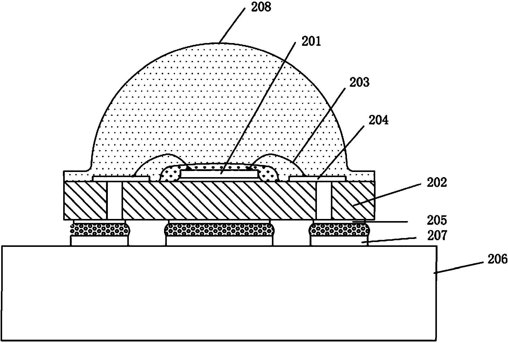
For example, the Chinese utility model patent with the authorized announcement number CN 201354966Y discloses a glass-packaged light-emitting diode. It is possible, but the heat dissipation of this package structure is not improved compared with the traditional package form. At the same time, due to the restriction of the electrode connection process using gold wires or wires, the reduction of the package size is restricted by the existence of gold wires or other wires.

Method used


Image

  • Substrate-free LED device and manufacturing method thereof
  • Substrate-free LED device and manufacturing method thereof
  • Substrate-free LED device and manufacturing method thereof

Examples


Embodiment 1

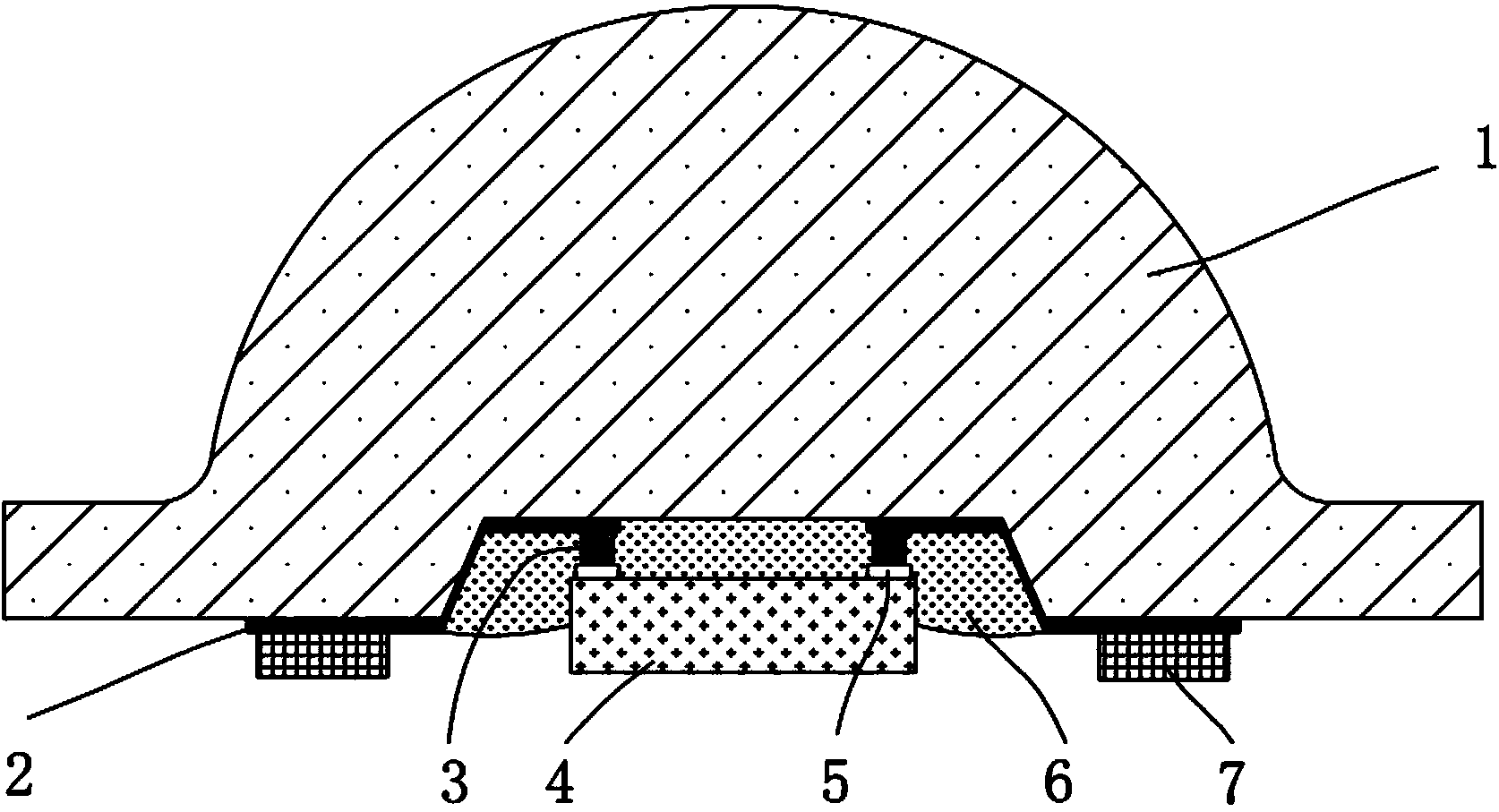
[0077] see image 3 Shown is a schematic structural view of an LED device with an integrated lens substrate in a typical embodiment of the present invention. The LED device includes a preformed lens 1 and at least one LED chip 4 (hereinafter referred to as chip). The lens 1 is provided with a metal or transparent conductive material wiring layer 2, and the chip has a metal electrode 5. The metal wiring layer 2 on the lens 1 (referred to as wiring 2) and the metal electrode 5 on the chip 4 are connected by a lead bump 3. The lens The external lead electrode 7 of the LED device (also referred to as "external electrode" for short below) is provided at a specific position of the wiring 2 on the LED device. Usually the chip is fixed in the groove at the bottom of the lens, and the groove is filled with transparent colloid 6 through the underfill process and cured, so that there are no air bubbles between the LED chip and the lens, reducing reflection loss. The lower surface of th...

Embodiment 2

[0095] The structure of a kind of LED device of the present embodiment can also refer to Figure 3-Figure 8 , and the fabrication process of the device is the same as in Example 1.

[0096] see Figure 10 Shown is a schematic diagram of a thermoelectric separation assembly of an LED device integrated with a lens substrate of the present invention. In this device, the chip 4 is a front-mounted chip, and its positive and negative electrodes are all on the upper surface of the chip. electrical connection. The lower surface of the chip 4 is directly connected to the top of the heat sink 1002 through thermal grease, eutectic soldering or other methods, so as to achieve low thermal resistance. The external electrodes 7 on the lens 1 are electrically connected to the outside through a PCB 1001 of a specific shape. The device is fixed on the heat sink 1002 through the pressing piece 1004 , the washer 1003 and the screw 1005 .

[0097] In addition, the electrical connection between t...

Embodiment 3

[0100] Please also see Figure 11-Figure 12 ,in Figure 11 It is a schematic top view diagram of an LED device (hereinafter referred to as the device) that includes a lens substrate integrated with multiple lens units. Figure 12 yes Figure 11 A schematic cross-sectional view of the device along the B-B' direction is shown.

[0101] The device is a multi-unit module integrated on the lens substrate 1101, wherein the main body of each unit lens can be designed as an aspheric surface according to the needs of the light type. The chips 4 in each unit module are connected in series / parallel through the wiring 1102 on the lens substrate 1101 . An external electrode is arranged on the edge of the lens substrate, and the external electrode cooperates with the lens substrate to form a plug 1103, which can form a plug-in connection with an external circuit through a matching socket. The lens substrate 1101 may be provided with a positioning hole 1104 . The device can be fixed on...


PUM


Abstract

The invention discloses a substrate-free LED device and a manufacturing method thereof. The LED device comprises an LED chip and a lens matched with the LED chip, wherein a conductive wiring layer is attached to the bottom of the lens, and an inner lead wire electrode and an outer lead wire electrode are arranged on the conductive wiring layer and are respectively and electrically connected with the LED chip and an external circuit. The manufacturing method of the substrate-free LED device comprises the steps of manufacturing the lens; manufacturing the conductive wiring layer at the bottom of the lens; connecting at least one of the electrodes of the LED chip with the conductive wiring layer on the corresponding lens. The substrate-free LED device is of the structure that the lens and a substrate are integrally arranged, cost is reduced, heat radiation effect is improved, the size of the device is decreased, meanwhile the reliability of the device is improved, and 360-deegree light emitting application is easily achieved.

Description

technical field [0001] The invention relates to a semiconductor light-emitting device, in particular to an LED packaging device with wiring on a lens, and belongs to the technical field of light-emitting diode manufacturing and assembly. Background technique [0002] Due to the advantages of high light efficiency, environmental protection, long life, and small size, LEDs are widely used in signals, display screens, mobile devices, monitors, televisions, etc., and gradually replace traditional light sources into the field of general lighting. [0003] Although the market penetration rate of LED continues to increase, its price is still relatively high compared with traditional lighting, which is an important factor hindering its popularization. [0004] The market also hopes that the reliability of LEDs will be further improved. Reducing the thermal resistance of packaging and assembly can effectively improve device performance and reliability. [0005] At the same time, in...

Claims


Application Information

Patent Timeline
Patent Type & Authority Applications(China)
IPC IPC(8): H01L33/48H01L33/58H01L33/62
CPCH01L33/48H01L33/005H01L33/58H01L33/62H01L2933/0033H01L2933/0058H01L2933/0066
Inventor 杨晓丽
Owner 杨晓丽
Learn More