SONOS (silicon oxide nitride oxide silicon) flash memory device and compiling method thereof

A flash memory device and substrate technology, which is applied in the manufacture of electric solid-state devices, semiconductor devices, semiconductor/solid-state devices, etc., can solve problems such as high current consumption, low channel hot electron injection efficiency, and high voltage, and achieve increased Effects of cell density, suppression of short channel effects, and reduction of readout errors

Active Publication Date: 2015-02-04
SHANGHAI HUALI MICROELECTRONICS CORP
View PDF8 Cites 9 Cited by
  • Summary
  • Abstract
  • Description
  • Claims
  • Application Information

AI Technical Summary

Problems solved by technology

[0006] However, the structure of the flash memory device disclosed in the above-mentioned documents has the following problems: in order to ensure a high channel hot electron generation rate, a high voltage must be applied to the drain terminal, and at the same time, in order to ensure a high hot electron injection efficiency, a high Voltage
Therefore, it is necessary to apply a high voltage to both the drain and the gate, which brings the problems of low channel hot electron injection efficiency and large current power consumption.

Method used


Image

  • SONOS (silicon oxide nitride oxide silicon) flash memory device and compiling method thereof
  • SONOS (silicon oxide nitride oxide silicon) flash memory device and compiling method thereof

Examples


Embodiment 1

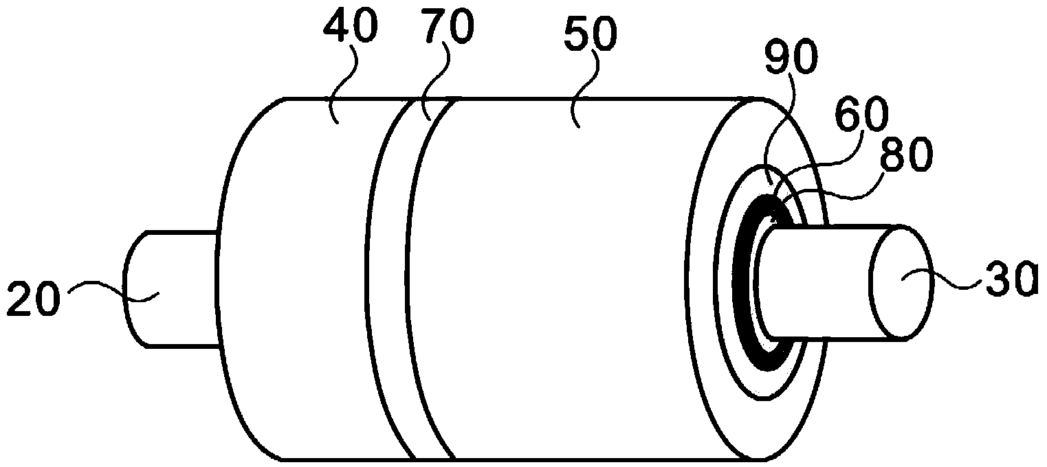
[0029] In this embodiment, the material of the first silicon gate 40 is polysilicon, its height is 90nm, and its length is 10nm; the material of the second silicon gate 50 is polysilicon, its height is 30nm, its length is 40nm; The material of the second oxide layer 80 is silicon dioxide with a thickness of 2 nm; the material of the third oxide layer 90 is silicon dioxide with a thickness of 8 nm. The manufacturing process of the device can be selected from the top-down technology compatible with the standard CMOS process.

[0030] In the SONOS flash memory device provided by the present invention, a cylindrical substrate structure is used, and the gate is covered on it. The use of a cylindrical structure can enable the voltage of the gate to better control the channel and suppress the short channel effect. , resist threshold voltage drift, reduce readout errors of flash memory, and at the same time, can effectively shorten the critical size of flash memory devices, increase t...

Embodiment 2

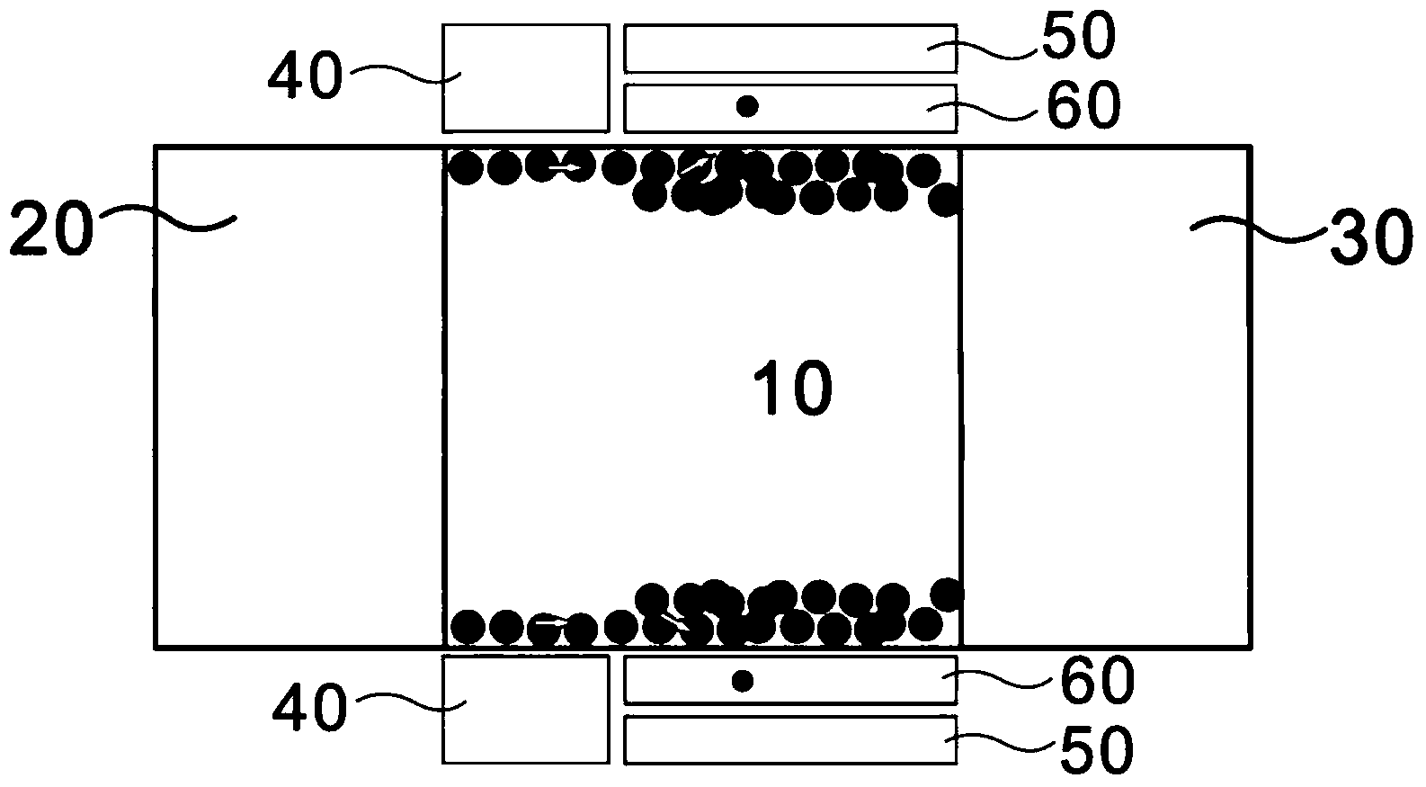
[0033] In this embodiment, when compiling the SONOS flash memory device, the voltage value applied to the first silicon gate 40 is equal to the threshold voltage value of the flash memory device, the voltage applied to the second silicon gate 50 is 8V, and the voltage applied to the drain terminal 30 is 4V. A voltage of 0V is applied to the source terminal 20 .

[0034] The compiling principle of the present invention is: when compiling a SONOS flash memory device, the voltage value applied to the first silicon gate 40 is equal to the threshold voltage value of the flash memory device, and a thinner channel electron layer is induced in the lower substrate region. The voltage applied to the second silicon gate 50 is greater than the threshold voltage of the flash memory device, and the voltage is coupled to the underlying silicon nitride layer 60 to induce a thicker channel electron layer in the lower channel electron layer. The voltage applied to the drain terminal 30 accelera...


PUM


Abstract

The invention provides an SONOS (silicon oxide nitride oxide silicon) flash memory device and a compiling method thereof. The SONOS flash memory device comprises a substrate of a cylinder structure and a grid electrode which wraps the middle of the substrate, wherein a source terminal and a drain terminal are respectively arranged at two ends of the substrate, the grid electrode comprises a first silicon gate and a second silicon gate which are parallel, a first oxidation layer is arranged between the first silicon gate and the second silicon gate, and a second oxidation layer arranged on the substrate, a silicon nitride layer arranged on the second oxidation layer and used to store electric charges and a third oxidation layer arranged on the silicon nitride layer are sequentially arranged between the second silicon gate and the substrate. The above structure of the SONOS flash memory device can restrain short channel effects and resist threshold voltage drifts, and simultaneously can effectively reduce the critical size of the SONOS flash memory device. The compiling method of the SONOS flash memory device assists in movement of thermion by adjusting voltage of the grid electrode and the drain terminal, provides sufficient oxidation layer crossing energy to complete compiling, improves compiling efficiency of the SONOS flash memory device, and reduces compiling electric current power consumption.

Description

technical field [0001] The invention relates to the field of semiconductor integrated circuits and its manufacture, in particular to a SONOS flash memory device and its compiling method. Background technique [0002] With the miniaturization and miniaturization of semiconductor storage devices, the traditional polysilicon second silicon gate storage is difficult to adapt to the development requirements of future storage because of the excessive thickness of the stack and the high requirements on the insulation of the tunnel oxide layer. Recently, SONOS (Polysilicon-Oxide-Nitride-Oxide-Silicon, Silicon-Oxide-Nitride-Oxide-Silicon) non-volatile memory devices based on silicon nitride with excellent insulating properties are known as the first Two-silicon gate memory has stronger charge storage capacity, easy miniaturization and simple process, and has been re-emphasized. [0003] SONOS, the English acronym for Silicon-Oxide-Nitride-Oxide-Silicon, is a non-volatile memory that...

Claims


Application Information

Patent Timeline
Patent Type & Authority Applications(China)
IPC IPC(8): H01L27/115H01L21/8247
Inventor 顾经纶
Owner SHANGHAI HUALI MICROELECTRONICS CORP
Why Eureka
Try Eureka