
Eureka
For R&D, Eureka makes reading and utilizing patents & technical documents easy.
Eureka AIR
Designed for self-driven R&D workflows. Generate viable solutions, solve complex R&D challenges, empower your innovation with AI.

Eureka Materials
Designed for material experts only. Revolutionize your material R&D, from search, analyze, to developing new materials.

TechResearch
Generate reliable direction feasibility study reports for your R&D in just a few steps.

TechSeek
Discover and master advanced knowledge NOW. Basics, ideas, possibilities, all at once.

TechMind
As an expert in R&D Theories, TechMind can generates customized viable solutions instantly.

TechRisk
Analyze your overall solution with one click, know your potential R&D risks in advance.

TechMonitor
Get weekly tech updates, stay abreast of the latest tech innovations and key insights.
Nonvolatile memory cell and memory
A non-volatile storage and storage circuit technology, which is applied in the field of semiconductor storage, can solve the problems of long time consumption and achieve good results and long data retention
- Summary
- Abstract
- Description
- Claims
- Application Information
AI Technical Summary
Problems solved by technology
Method used
Image

Examples
Embodiment 1
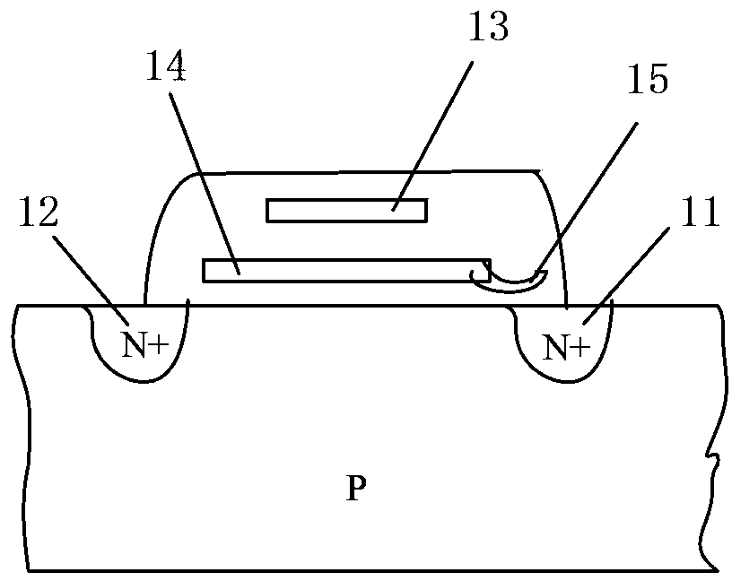
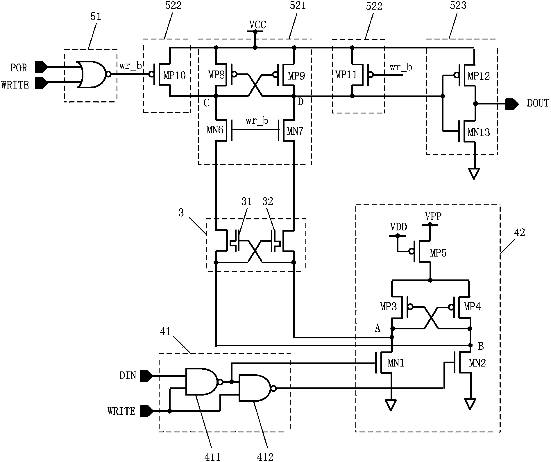
[0022] image 3 It is a schematic structural diagram of a non-volatile memory unit provided by Embodiment 1 of the present invention. Such as image 3 As shown, the non-volatile storage unit may include: a differential storage circuit 3 , a write circuit and a read circuit.
[0023] Among them, the input terminal of the data to be stored in the write circuit is used to input the data DIN to be stored, the input terminal of the read and write signal of the write circuit is used to input the read and write signal WRITE, and the write circuit is used to read and write data according to the input data DIN and the input to be stored. The write signal WRITE outputs a storage control signal to control the differential storage circuit 3 to store data; the input end of the differential storage circuit 3 is connected to the write circuit, and the differential storage circuit 3 includes two sets of storage components. In one storage cycle, one set The storage component performs a progr...
Embodiment 2
[0050] Figure 6 A schematic structural diagram of the memory provided by Embodiment 2 of the present invention, such as Figure 6 As shown, the memory includes a read-write controller and a plurality of storage units, and the storage units adopt the non-volatile storage units provided by the above-mentioned embodiments to store and read data. According to the data and control information input from the outside, the read-write controller generates corresponding signals and outputs them to each storage unit to complete the data access. After the data is written, it can output the data stored in all storage units in parallel. Without an additional sense amplifier circuit, for the non-volatile memory unit in the above embodiment, the read-write controller at least generates data to be stored and read-write signals. The connection relationship among the storage units may refer to the common connection manner in the prior art, which is not limited in this embodiment.
PUM
 Abstract
Description
Claims
Application Information
 - R&D Engineer
- R&D Manager
- IP Professional
- Industry Leading Data Capabilities
- Powerful AI technology
- Patent DNA Extraction
Browse by: Latest US Patents, China's latest patents, Technical Efficacy Thesaurus, Application Domain, Technology Topic, Popular Technical Reports.
© 2024 PatSnap. All rights reserved.Legal|Privacy policy|Modern Slavery Act Transparency Statement|Sitemap|About US| Contact US: help@patsnap.com