Manufacturing method of groove type MOS (Metal Oxide Semiconductor) transistor with electrostatic discharge protection circuit

A technology for MOS transistors and protection circuits, which is applied in the field of trench MOS transistor manufacturing, can solve problems such as metal etching residues and difficulties in subsequent process planarization, and achieve the goals of improving flatness, reducing residual risks, and shortening the process flow Effect

Active Publication Date: 2015-02-11
SHANGHAI HUAHONG GRACE SEMICON MFG CORP
View PDF3 Cites 19 Cited by
  • Summary
  • Abstract
  • Description
  • Claims
  • Application Information

AI Technical Summary

Problems solved by technology

In addition, in the structure of a typical power MOS transistor with electrostatic discharge protection circuit, there is a height difference between the active area and the electrostatic protection area, forming steps, which will cause certain difficulties for the planarization of the subsequent process, and there will be residual risks in metal etching

Method used


Image

  • Manufacturing method of groove type MOS (Metal Oxide Semiconductor) transistor with electrostatic discharge protection circuit
  • Manufacturing method of groove type MOS (Metal Oxide Semiconductor) transistor with electrostatic discharge protection circuit
  • Manufacturing method of groove type MOS (Metal Oxide Semiconductor) transistor with electrostatic discharge protection circuit

Examples


Embodiment Construction

[0033] In order to have a more specific understanding of the technical content, characteristics and effects of the present invention, now in conjunction with the illustrated embodiment, the details are as follows:

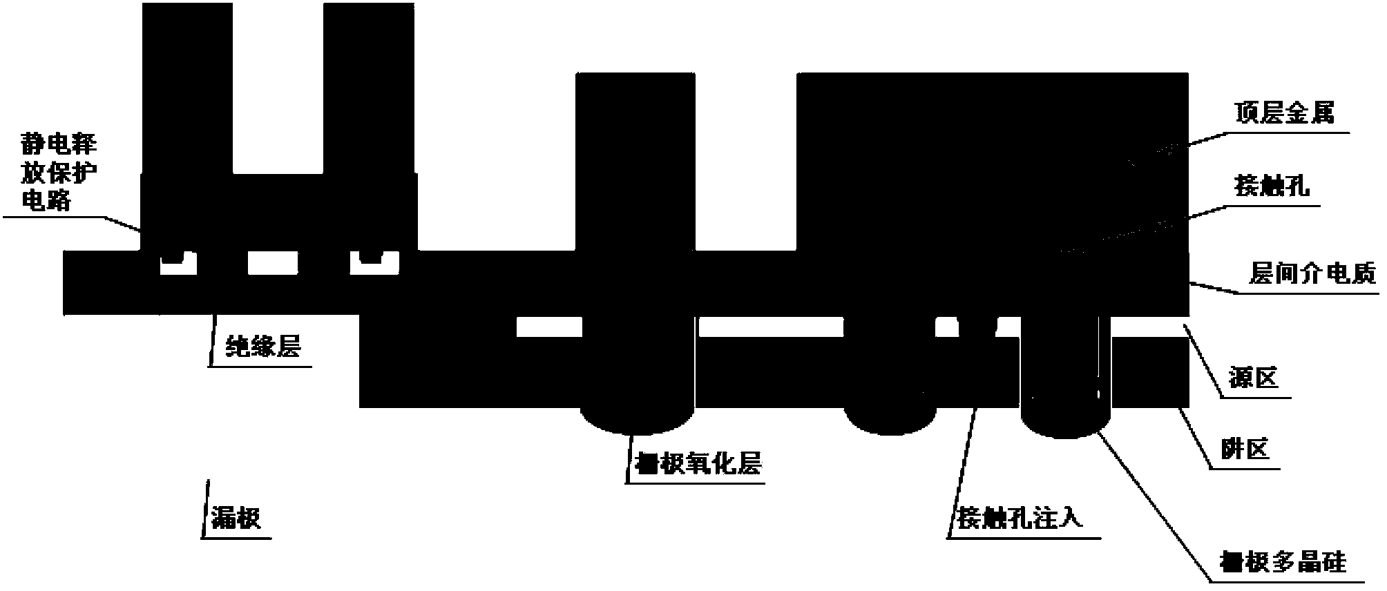
[0034] The trench power MOS transistor with electrostatic discharge protection circuit of the present invention improves the gate channel and dielectric layer structure on the basis of the original structure, and its specific process realization process is as follows:

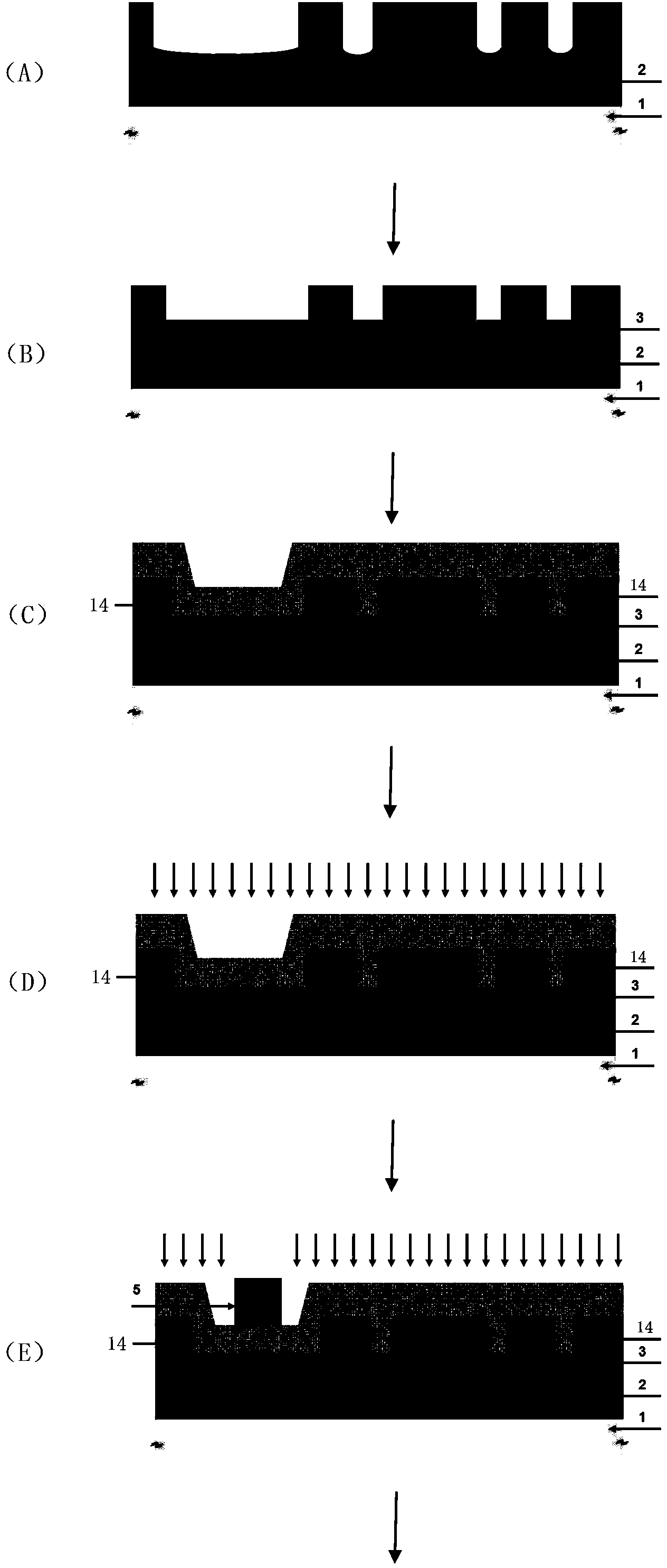
[0035] Step 1, grow an epitaxial layer 2 on the substrate 1, and then etch and form trenches on the epitaxial layer 2, such as image 3 (A) shown.

[0036] Step 2: Deposit a layer of dense silicon dioxide in the trench using atmospheric pressure chemical vapor deposition, and then etch back to form a 3000-4000 angstrom thick gate oxide 3 at the bottom of the trench, such as image 3 (B) shown. This layer of thick gate oxide 3 is used as an insulating layer between the electrostatic discharge prote...


PUM


Abstract

The invention discloses a manufacturing method of a groove type MOS (Metal Oxide Semiconductor) transistor with an electrostatic discharge protection circuit. The manufacturing method comprises the following steps: (1) carrying out epitaxial growth and groove etching; (2) carrying out groove bottom thick grid oxygen deposition and back etching; (3) carrying out non-doped polycrystalline silicon deposition; (4) carrying out primary polycrystalline injection; (5) carrying out secondary polycrystalline injection; (6) carrying out polycrystalline silicon back etching to form grid electrode polycrystalline silicon and electrostatic discharge protection circuit polycrystalline silicon; (7) carrying out trap injection; (8) carrying out source injection. An inter-layer medium layer, a contact hole, top layer metal and back metal are formed in a follow-up step according to a conventional process. On the basis of a traditional process, a groove bottom thick grid oxygen structure is used as an insulating layer between the electrostatic discharge protection circuit and a groove power device, and then the polycrystalline deposition is carried out; photoetching partitioned injection and back etching are combined to form groove polycrystalline silicon and the electrostatic discharge protection circuit polycrystalline silicon; one active region photoetching layer and primary polycrystalline silicon deposition and back etching are reduced, so that the technological process is shortened.

Description

technical field [0001] The invention relates to the field of integrated circuit manufacturing, in particular to a method for manufacturing a trench MOS transistor with an electrostatic discharge protection circuit. Background technique [0002] In a semiconductor integrated circuit, the structure of a typical power MOS transistor with an electrostatic discharge protection circuit is as follows: figure 1 As shown, an insulating area is specially made for the deposition of polysilicon for the electrostatic discharge protection circuit. The insulating region is generally formed by thermal oxygen deposition, which has a certain degree of consumption of the epitaxial layer. Therefore, in order to achieve a one-click breakdown voltage device, the epitaxial layer usually used is more than that required by ordinary power MOS transistors without electrostatic discharge protection circuits. The epitaxial layer is thicker. In addition, in the structure of a typical power MOS transist...

Claims


Application Information

Patent Timeline
Patent Type & Authority Applications(China)
IPC IPC(8): H01L21/336
Inventor 柯行飞朱熹
Owner SHANGHAI HUAHONG GRACE SEMICON MFG CORP
Why Eureka
Try Eureka