Novel method for manufacturing LED chips

A technology of LED chips and manufacturing methods, which is applied in semiconductor/solid-state device manufacturing, semiconductor devices, electrical components, etc., can solve the problems of high price of LED products, inconvenience in large-scale production, and poor lithography stations, etc. The effect of chemical production, process defect reduction and production cycle shortening

Active Publication Date: 2015-02-18
SHANDONG CHENGLIN PHOTOELECTRIC TECH +1
View PDF4 Cites 1 Cited by
  • Summary
  • Abstract
  • Description
  • Claims
  • Application Information

AI Technical Summary

Problems solved by technology

[0013] However, the above-mentioned four-lead process is not conducive to cost saving, and the production cycle is long, which is not convenient for large-scale production. At the same time, the poor photolithography station is the main factor affecting the yield. Due to the four-lead process, too many times of photolithography, the yield rate Low, which leads to the higher price of LED products than ordinary optical devices, which limits its large and rapid development

Method used


Image

  • Novel method for manufacturing LED chips
  • Novel method for manufacturing LED chips
  • Novel method for manufacturing LED chips

Examples


Embodiment Construction

[0050] In order to make the purpose, technical solutions and advantages of the present invention clearer and for those skilled in the art to better understand the technical solutions of the present invention, the present invention will be described in further detail below in conjunction with specific embodiments and with reference to the accompanying drawings. Apparently, the described embodiments are only some of the embodiments of the present invention, but not all of them. Based on the embodiments of the present invention, all other embodiments obtained by persons of ordinary skill in the art without creative efforts fall within the protection scope of the present invention. Also, in the following description, descriptions of well-known structures and techniques are omitted to avoid unnecessarily obscuring the concept of the present invention.

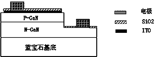
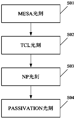
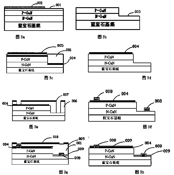
[0051] see Figure 4 , is a structural schematic diagram of a method for manufacturing a novel LED chip provided by an embodiment...


PUM


Abstract

The invention discloses a novel method for manufacturing LED chips. The novel method includes performing MESA photoetching and NP (negative and positive) photoetching, and particularly includes performing vacuum evaporation on the surfaces of epitaxial slices to obtain ITO (indium tin oxide) layers, then coating photoresist on the surfaces of the epitaxial slices, then performing MESA photoetching on the epitaxial slices to obtain photoresist layers with MESA pattern layers, etching ITO of the ITO layers and downwardly etching the surfaces of the epitaxial slices; removing the photoresist layers with the MESA pattern layers; performing vacuum evaporation on steps of the ITO layers and N-GaN layers to obtain SiO<2> layers, coating photoresist on the steps of the ITO layers and the N-GaN layers, and performing NP photoetching on the photoresist layers to obtain photoresist layers with NP patterns; etching the SiO<2> layers; forming P electrodes and N electrodes in regions obtained after the SiO<2> layers are etched; removing the photoresist layers with the NP pattern layers. The novel method has the advantages that the production cost can be effectively reduced, the production cycle can be shortened, and the yield can be increased.

Description

technical field [0001] The invention relates to the field of LED manufacture and application, in particular to a method for manufacturing a novel LED chip. Background technique [0002] LED chip is an energy-saving and environmentally friendly product. It is a light-emitting diode. Its working principle is to convert electrical energy into light energy. It has low energy consumption, high brightness, and long life. Its development is very promising, and its initial application is only in experimental research and development. stage. In recent years, with the development of science and technology, its manufacturing process has gradually matured, and it has gradually entered mass production in factories, and its application has become more extensive. [0003] The finished structure of the LED chip is as follows figure 1 shown. The production process of LED chips is to make a single chip on an epitaxial wafer (2 inches). The size of a single chip is small and cannot be disti...

Claims


Application Information

Patent Timeline
Patent Type & Authority Applications(China)
IPC IPC(8): H01L33/00
CPCH01L21/0274H01L33/007
Inventor 高俊民许键吴伟东李爱玲成涛王占伟于海莲
Owner SHANDONG CHENGLIN PHOTOELECTRIC TECH
Why Eureka
Try Eureka