Interface oxygen vacancy based stable-storage resistive random access memory achieving method

A technology of resistive storage and oxygen vacancies, which is applied in the direction of electrical components, etc., can solve the problems that Flash storage technology cannot meet the requirements of ultra-high storage density, the programming voltage cannot be reduced proportionally, and the performance of device charge retention is reduced. Resistive storage performance, simple structure, stable and uniform thickness

Inactive Publication Date: 2015-03-04
ZHEJIANG SCI-TECH UNIV
View PDF4 Cites 3 Cited by
  • Summary
  • Abstract
  • Description
  • Claims
  • Application Information

AI Technical Summary

Problems solved by technology

Although Flash technology has achieved great success in the market, it is limited by its own storage mechanism. With the further reduction of feature size, the development of this technology faces many difficulties.
On the one hand, its programming voltage cannot be reduced proportionally; on the other hand, as the device size continues to shrink, the thickness of the tunnel oxide layer becomes thinner and thinner, and the charge leakage will become more and more serious, which makes the charge retention performance of the device decrease.
Therefore, Flash storage technology cannot meet the requirements of the rapid development of information technology for ultra-high storage density.

Method used


Image

  • Interface oxygen vacancy based stable-storage resistive random access memory achieving method
  • Interface oxygen vacancy based stable-storage resistive random access memory achieving method
  • Interface oxygen vacancy based stable-storage resistive random access memory achieving method

Examples


Embodiment 1

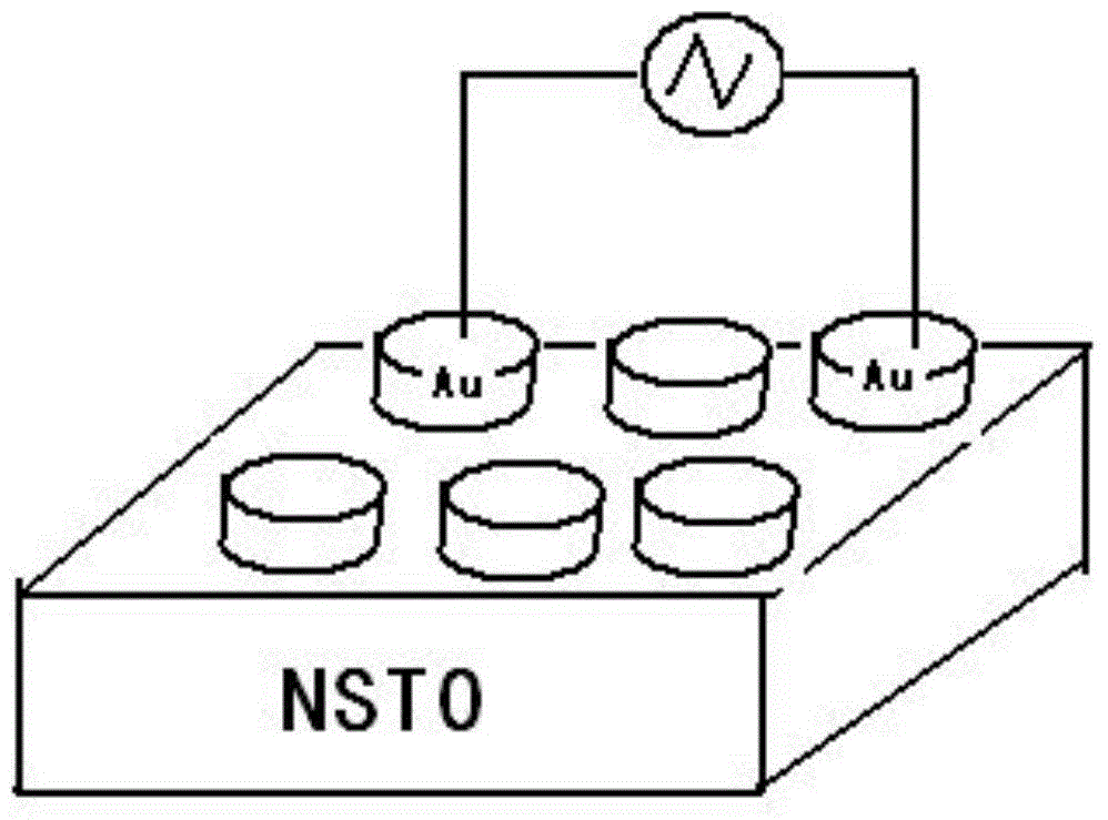
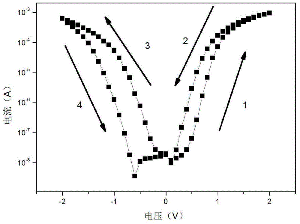
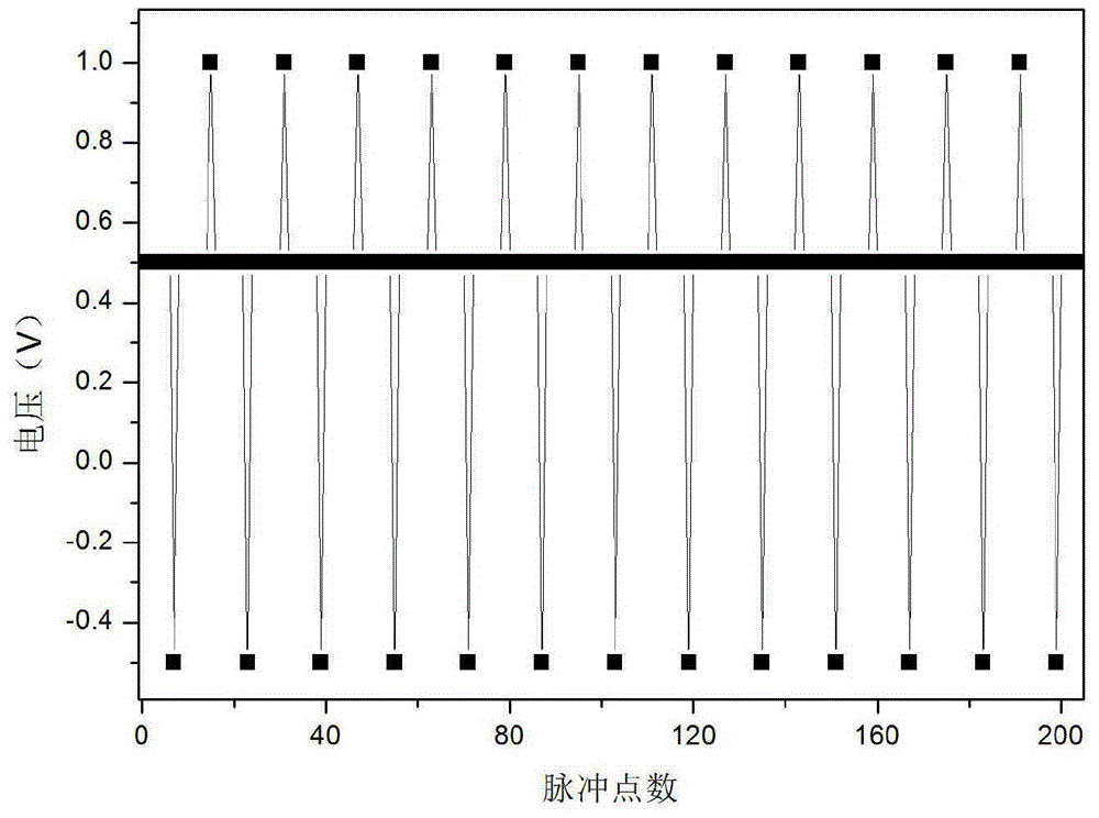
[0023] Take a piece of single crystal SrTiO containing Nb with a size of 10mm×5mm×0.5mm 3 substrate, where the single crystal SrTiO 3 The substrate contains 0.7% Nb, which were ultrasonically cleaned in deionized water, acetone, deionized water, ethanol, and deionized water for 5 min, 15 min, 5 min, 15 min, and 5 min, respectively, and dried naturally. Cover the cleaned substrate with a mask plate, place it in the vacuum chamber of a magnetron sputtering apparatus, and use radio frequency magnetron sputtering method on the exposed Nb-containing single crystal SrTiO 3 A metal gold (Au) film with a thickness of 100nm and a diameter of 1mm is sputtered on the substrate. The schematic diagram of the device structure is shown in figure 1 . The vacuum degree during the RF magnetron sputtering method used is 9.7×10 -4 pa, the sputtering air pressure is 0.8Pa, the sputtering time is 9min, the sputtering power is 60W, and the target base distance is 5cm. Two metal gold (Au) electro...

Embodiment 2

[0025] Same as embodiment 1, get a piece of Nb-containing single crystal SrTiO with a size of 10mm × 5mm × 0.5mm 3 A substrate in which the single crystal SrTiO 3 The substrate contains Nb with a mass content of 0.5%, and it is ultrasonically cleaned in deionized water, acetone, deionized water, ethanol, and deionized water for 5 min, 15 min, 5 min, 15 min, and 5 min, respectively, and dried naturally. Cover the cleaned substrate with a mask plate, place it in the vacuum chamber of a magnetron sputtering apparatus, and use radio frequency magnetron sputtering method on the exposed Nb-containing single crystal SrTiO 3 A metal gold (Au) film with a thickness of 100nm and a diameter of 1mm is sputtered on the substrate. The schematic diagram of the device structure is shown in figure 1 . The vacuum degree during the RF magnetron sputtering method used is 9.7×10 -4 pa, the sputtering air pressure is 0.8Pa, the sputtering time is 9min, the sputtering power is 60W, and the target...


PUM


Abstract

The invention discloses an interface oxygen vacancy based stable-storage resistive random access memory achieving method and relates to a Schottky contact based method for achieving resistive random access memories which is optimal in storage performance and simple in structure. According to the method, a magnetron sputtering method is used for sputtering metal Au film on an Nb: SrTiO3 mono-crystal substrate to obtain memories in an Au/Nb: Sr TiO3/Au plane structure, and accordingly, the stable-maintaining resistive random access memory performance is obtained. The method has the advantages that resistive random access memories are produced by plating Au on a mono-crystal Nb: SrTiO3 substrate through magnetron sputtering, the production process is achieved through one step, the memory production process is simple, other complex steps are not needed, and resistive random access memories are simple in structure and applicable to industrial production. The performance test result shows that compared with prior inventions, a good maintaining performance is provided, which is one of key factors determining the memory performance.

Description

technical field [0001] The invention relates to a preparation method of a resistive memory unit device based on an Au / NSTO / Au double Schottky structure to realize stable resistive memory, specifically refers to a single crystal with metal Au as an electrode and 0.7wt% Nb doped SrTiO 3 The realization of the stable resistive memory performance of the heterostructure as the resistive layer material. technical background [0002] With the rapid development of computer technology, the Internet and new portable electronic products in today's society, people have higher and higher requirements for information memory performance, which urgently requires greater progress in memory materials and technologies. Although Flash technology has achieved great success in the market, due to the limitation of its own storage mechanism, the development of this technology is facing many difficulties as the feature size is further reduced. On the one hand, its programming voltage cannot be red...

Claims


Application Information

Patent Timeline
Patent Type & Authority Applications(China)
IPC IPC(8): H01L45/00
Inventor 李培刚汪鹏超王顺利陈瑞品朱志艳沈静琴
Owner ZHEJIANG SCI-TECH UNIV
Why Eureka
Try Eureka