Input interface integrated circuit and input interface circuit thereof
A technology of input interface circuit and input terminal, which is applied in the direction of logic circuit connection/interface layout, etc., and can solve the problems of increasing circuit power consumption and system power consumption
- Summary
- Abstract
- Description
- Claims
- Application Information
AI Technical Summary
Problems solved by technology
Method used
Image

Examples
Embodiment 1
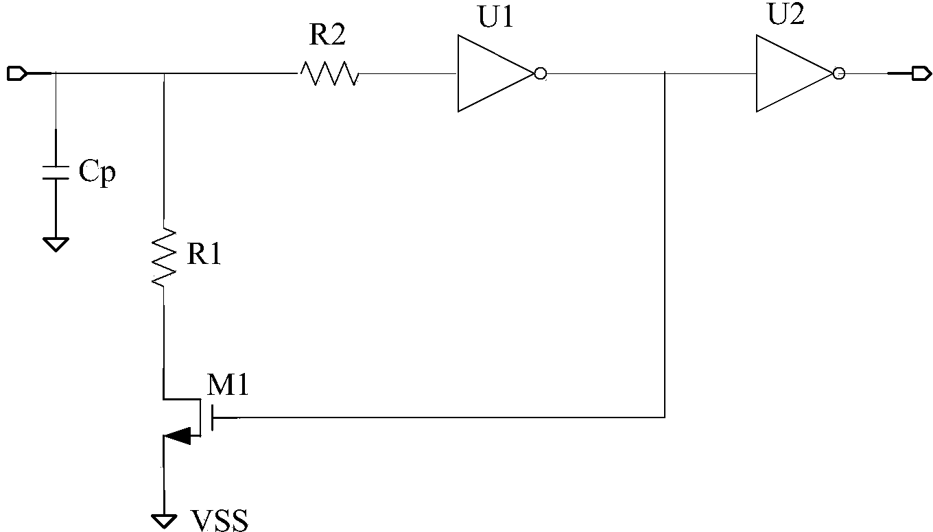
[0041] Such as figure 1 as shown, figure 1 It is a schematic diagram of an input interface circuit provided in Embodiment 1 of the present application. The input interface circuit includes: a parasitic capacitor Cp, a first resistor R1, a second resistor R2, a first MOS transistor M1, a first inverter U1 and a second inverter U2.
[0042] Wherein, the input terminal of the input interface circuit is grounded through the parasitic capacitance Cp, and at the same time connected to the drain of the first MOS transistor M1 through the first resistor R1, the source of the first MOS transistor M1 is grounded or powered, and the gate of the first MOS transistor M1 The pole is connected to the output terminal of the input interface circuit through the second inverter U2;
[0043] The input terminal of the input interface circuit is also connected to the output terminal of the input interface circuit through the second resistor R2, the first inverter U1 and the second inverter U2 in ...
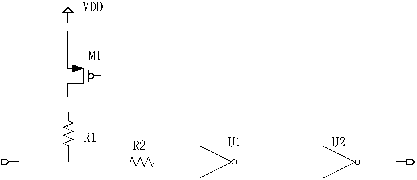
Embodiment 2
[0049] The basic principle of the input interface circuit provided in this application is based on a characteristic of CMOS circuits, that is, whether it is an N-type or a P-type MOS transistor, when they are in the cut-off state, when there is a voltage drop from the drain to the source, they will The leakage current from the drain to the source is determined by the basic principle of the device. The magnitude of the leakage current is closely related to the voltage drop from the drain to the source and the temperature. Generally speaking, the larger the voltage drop from the drain to the source, the larger the leakage current, and the higher the temperature, the larger the leakage current. Due to the existence of this leakage current, the charge accumulated on the drain of the MOS transistor will be converted into leakage current and released to the source. The voltage drop from the drain level to the source level will decrease, which is a slow and continuous process. Our ci...
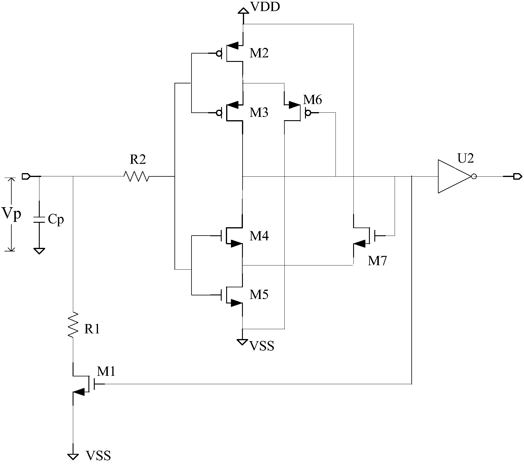
Embodiment 3
[0067] The input port generally has three connection states, that is, the input port is suspended, the input port is pulled to the power supply or ground by an external resistor, and the input port is driven by an external circuit.
[0068] Assuming that the input port is floating, when the power supply voltage is applied to this circuit, the power supply rise curve is unknown, and if it is powered by multiple power supplies, the timing of the power supply is also random, these factors lead to the instantaneous rise of the power supply In the state process, the charge accumulation process on the capacitor Cp is unpredictable, which directly causes the voltage on Cp to be random.
[0069] In most cases, this voltage cannot reach the upper threshold voltage of the Schmitt trigger. Among them, the specific threshold voltage and hysteresis interval are closely related to the specific implementation of the circuit. The selection of circuit parameters can determine the hysteresis ch...
PUM
 Abstract
Description
Claims
Application Information