A new welding device and method for soldering components on ceramic substrates

A welding device and ceramic substrate technology, applied in the direction of assembling printed circuits with electrical components, auxiliary devices, welding equipment, etc., can solve the problems that affect the welding quality and product performance, the operator's proficiency is greatly affected, and the welding consistency is poor. Achieve the effect of ensuring stability and reliability of solder joints, good operability, and reducing possibility

Inactive Publication Date: 2016-08-24
THE 41ST INST OF CHINA ELECTRONICS TECH GRP
View PDF7 Cites 0 Cited by
  • Summary
  • Abstract
  • Description
  • Claims
  • Application Information

AI Technical Summary

Problems solved by technology

During the cooling process, any small displacement of the components to be welded, especially those with small dimensions, will greatly reduce the welding quality
[0004] The main problem of the existing soldering process is: when the size of the components on the substrate is small (the lateral dimension is less than 1mm×1mm), the size of the components is similar to the size of the solder paste, any slight movement of the substrate during the cooling process will cause the components to shake, and the soldering As a result, the dots will appear in various irregular shapes, and the device will appear inverted, twisted, removed from the pad, and virtual soldering. Quality and product performance; at the same time, because the welding process is greatly affected by the proficiency of the operator, the welding consistency is poor and the welding efficiency is low

Method used


Image

  • A new welding device and method for soldering components on ceramic substrates
  • A new welding device and method for soldering components on ceramic substrates
  • A new welding device and method for soldering components on ceramic substrates

Examples


Embodiment Construction

[0035] The present invention is described in detail below in conjunction with accompanying drawing:

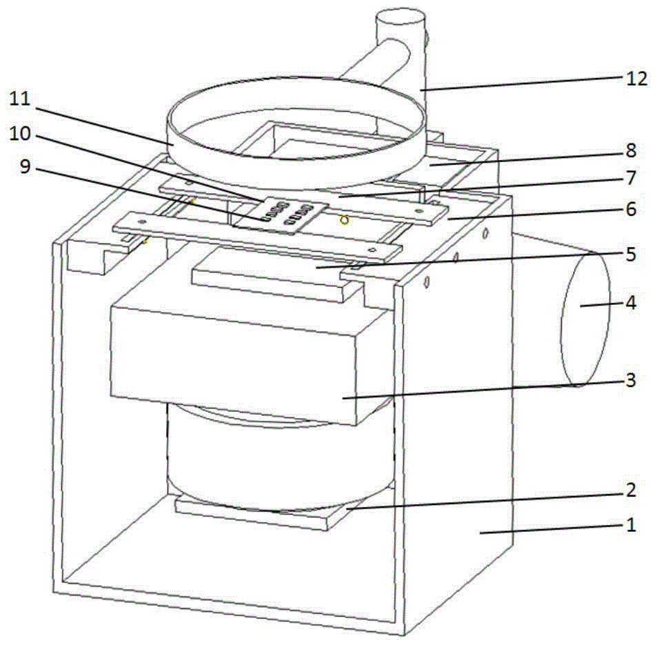
[0036] Such as figure 1 As shown, the device can be used to solder components on various ceramic substrates. Compared with traditional welding heating devices, this device has better welding quality and higher welding efficiency. A new welding device for soldering components on a ceramic substrate, the device is composed of four parts: a casing 1, a heating assembly, a lifting assembly, a carrying assembly and an observation assembly. The bottom of the shell is connected with the heating platform 3 of the heating assembly through the connecting plate 2 .

[0037]Heating component: the heating component is composed of a heating platform 3, a power supply and a heat transfer block 5, and the power supply is connected to the heating platform through wires to adjust the temperature of the heating platform. The current general-purpose heating table 3 is limited by the thermal co...


PUM


Abstract

The invention discloses a novel welding device and method for soldering components on a ceramic substrate. The device comprises a heating component, a lifting component and a bearing component; the heating component comprises a heating table; the heating table is connected with a power source through a wire, and the heating table transmits heat to the bottom of the substrate to be heated through a heat transmission block; the heating table is in contact with or is separated from the substrate to be heated through the lifting component; a gear transmission mechanism is embedded into the lifting component; a rotary knob can be rotated to enable the heating table to ascend and descend; the bearing component is arranged on the heat transmission block and comprises two bearing plates and two adjusting blocks; the adjusting blocks are arranged at the opposite positions of the plane on the upper portion of a shell; sliding grooves are formed in the adjusting blocks; the two ends of each bearing plate are placed on the sliding grooves in the adjusting blocks on the opposite positions respectively; and the distance between the bearing plates is adjustable. The device is simple in structure, good in operability, easy to produce and capable of being used for a long time, and the welding efficiency can be improved to be greatest extent.

Description

technical field [0001] The invention relates to a novel welding device and method for soldering components on a ceramic substrate. Background technique [0002] Ceramic substrate refers to a special process board in which copper foil is directly bonded to the surface of an alumina (Al2O3) or aluminum nitride (AlN) ceramic substrate (single or double-sided) at high temperature. The produced ultra-thin composite substrate has excellent electrical insulation performance, high thermal conductivity, excellent solderability and high adhesion strength, and can etch various patterns like a PCB board, and has a large current-carrying capacity. ability. Therefore, ceramic substrates have become the basic materials for high-power power electronic circuit structure technology and interconnection technology. And more packaging technologies based on ceramic materials are also widely used, such as low temperature co-fired ceramic (Low Temperature Co-fired Ceramic LTCC) technology and hig...

Claims


Application Information

Patent Timeline
Patent Type & Authority Patents(China)
IPC IPC(8): B23K3/08H05K3/34
CPCB23K3/08B23K3/087H05K3/34
Inventor 王文强路波霍建东郑如松赵秉玉张强
Owner THE 41ST INST OF CHINA ELECTRONICS TECH GRP
Why Eureka
Try Eureka