Supercharge Your Innovation With Domain-Expert AI Agents!

Layout design of MOSFET with multiple interdigital grid electrode structures

A gate structure and layout design technology, which is applied in the direction of electrical components, circuits, semiconductor devices, etc., can solve the problems of reducing the cut-off frequency and oscillation frequency of the device, affecting the radio frequency performance of the device, etc., to reduce parasitic capacitance, improve integration, volume Effect of reduced contact area

Active Publication Date: 2015-03-11
SHANGHAI INST OF MICROSYSTEM & INFORMATION TECH CHINESE ACAD OF SCI
View PDF5 Cites 4 Cited by
  • Summary
  • Abstract
  • Description
  • Claims
  • Application Information

AI Technical Summary

Problems solved by technology

However, the body contact technology introduces additional parasitic parameters, such as the influence of parasitic resistance and parasitic capacitance, which will affect the RF performance of the device, especially the oscillation frequency reduces the cut-off frequency and oscillation frequency of the device. How to improve the frequency characteristics of the device has always been The focus of research on device work

Method used


Image

  • Layout design of MOSFET with multiple interdigital grid electrode structures
  • Layout design of MOSFET with multiple interdigital grid electrode structures
  • Layout design of MOSFET with multiple interdigital grid electrode structures

Examples


Embodiment Construction

[0039] Embodiments of the present invention are described below through specific examples, and those skilled in the art can easily understand other advantages and effects of the present invention from the content disclosed in this specification. The present invention can also be implemented or applied through other different specific implementation modes, and various modifications or changes can be made to the details in this specification based on different viewpoints and applications without departing from the spirit of the present invention.

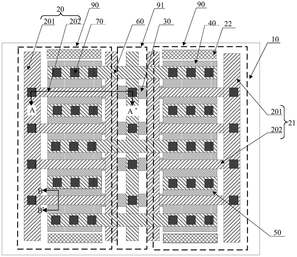
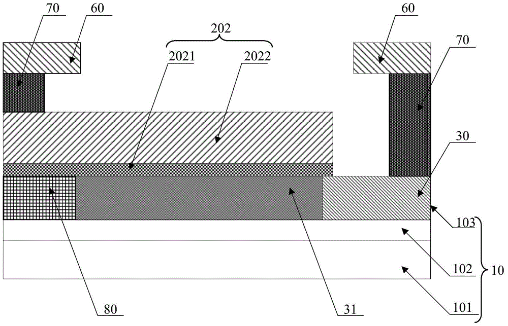
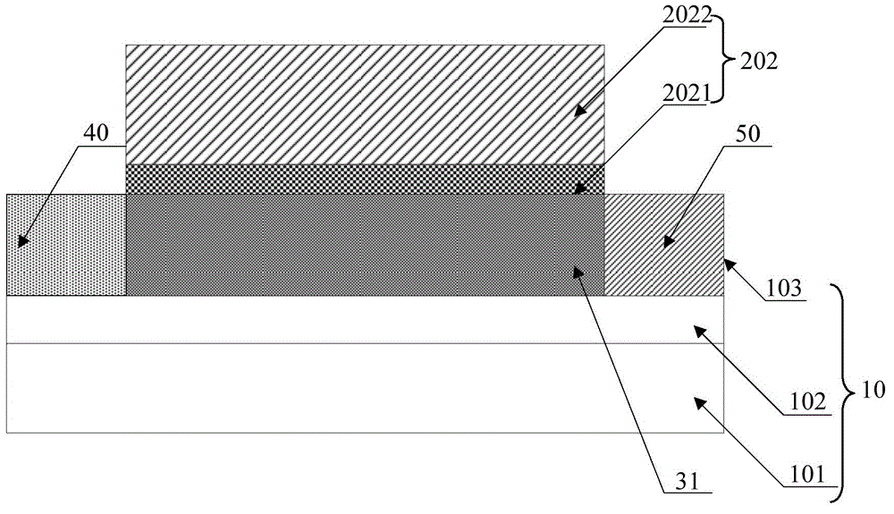
[0040] see Figure 1 to Figure 3 . It should be noted that the diagrams provided in this embodiment are only schematically illustrating the basic concept of the present invention, although only the components related to the present invention are shown in the diagrams rather than the number, shape and Dimensional drawing, the type, quantity and proportion of each component can be changed arbitrarily during actual implementation, and t...


PUM


Abstract

The invention provides a layout deign of a MOSFET (Metal-Oxide-Semiconductor Field Effect Transistor) with multiple interdigital grid electrode structures. The MOSFET comprises a semiconductor substrate, a first interdigital grid electrode structure, a second interdigital grid electrode structure, a body contact zone, a source zone and a drain zone; and the body contact zone is shared by the first interdigital grid electrode structure and the second interdigital grid electrode structure. The body contact zone is shared, so that the utilization rate of the body contact zone can be improved and the parasitic capacitance can be reduced. Compared with an ordinary body contact device, the active zone has high utilization rate; under the same total grid width condition, the area of the body contact zone is reduced by half and the integration level is improved. The middle body zone is shared by the active zones at two sides, so that the occupied area of metal connecting wires is reduced and the parasitic capacitance can be reduced. The parallel connection of grid electrodes at two sides is realized without increasing wiring difficulty and the resistance of the grid electrodes is reduced. The parallel connection of the drain electrodes at two sides is realized without increasing wiring difficulty and the resistance of the drain electrodes is reduced. The design method of the layout structure of devices has a certain application value in the radio frequency circuit field.

Description

technical field [0001] The invention relates to the technical field of semiconductor devices, in particular to a layout design of a MOSFET with a multi-finger gate structure. Background technique [0002] With the continuous development of semiconductor technology, metal-oxide-semiconductor field-effect transistors (MOSFETs) are widely used in integrated circuit design. Silicon-on-insulator technology (SOI), due to the buried oxide layer, has low parasitic capacitance, and the direct frequency of the device is higher than that of bulk silicon technology. Moreover, SOI technology realizes full dielectric isolation of a single device, eliminating the latch-up effect, and Low leakage current, very suitable for low power consumption, high performance applications. With the application of high-resistance substrates, it is possible to integrate high-quality integrated inductors on insulating silicon substrates, and the integration level is higher. At the same time, because of its...

Claims


Application Information

Patent Timeline
Patent Type & Authority Applications(China)
IPC IPC(8): H01L29/78H01L29/06H01L29/10H01L29/423
CPCH01L29/0684H01L29/42356H01L29/78
Inventor 陈静吕凯罗杰馨柴展何伟伟黄建强王曦
Owner SHANGHAI INST OF MICROSYSTEM & INFORMATION TECH CHINESE ACAD OF SCI
Features
  • R&D
  • Intellectual Property
  • Life Sciences
  • Materials
  • Tech Scout
  • Unparalleled Data Quality
  • Higher Quality Content
  • 60% Fewer Hallucinations
Learn More