Photoelectric device manufacturing system with online detection function

A technology for optoelectronic devices and preparation systems, which is applied in the manufacturing/processing of organic semiconductor devices, electric solid state devices, semiconductor/solid state device manufacturing, etc. performance of organic semiconductor materials research and other issues, to achieve the effect of improving accuracy and realizing real-time measurement

Inactive Publication Date: 2015-03-11
TECHNICAL INST OF PHYSICS & CHEMISTRY - CHINESE ACAD OF SCI
View PDF10 Cites 0 Cited by
  • Summary
  • Abstract
  • Description
  • Claims
  • Application Information

AI Technical Summary

Problems solved by technology

At present, in countries with rapid development of OLED industrialization, such as Japan, the United States, South Korea, and Taiwan, China, there are commercial OLED preparation equipment, but the preparation and performance evaluation system of organic thin film materials and devices is independent, often After the device is packaged, several different detection systems are used to test its photoelectric performance. Therefore, if there are minor mistakes in the packaging process, it is difficult to guarantee the accuracy of the photoelectric performance test results.
In addition, in the research stage of organic thin film materials, it is often not necessary to make it into a device and then test its performance
The quantum efficiency, emission spectrum, and chromaticity of organic thin film materials are easily affected by oxygen, water, and ultraviolet light. The conventional off-line photoelectric performance detection error is large, which greatly hinders the research of high-performance organic semiconductor materials.
[0012] In summary, neither the organic thin film preparation system nor the optoelectronic device preparation system in the prior art can realize the online detection of the organic thin film or optoelectronic device in a vacuum environment, and it is necessary to take the prepared organic thin film or optoelectronic device out of the preparation system. , and then get the performance of the organic thin film or optoelectronic device to be tested in the special testing equipment. The influence of oxygen, water vapor and ultraviolet light

Method used


Image

  • Photoelectric device manufacturing system with online detection function
  • Photoelectric device manufacturing system with online detection function
  • Photoelectric device manufacturing system with online detection function

Examples


Embodiment Construction

[0032] The content of the invention of the present invention will be further described below in conjunction with the accompanying drawings and embodiments.

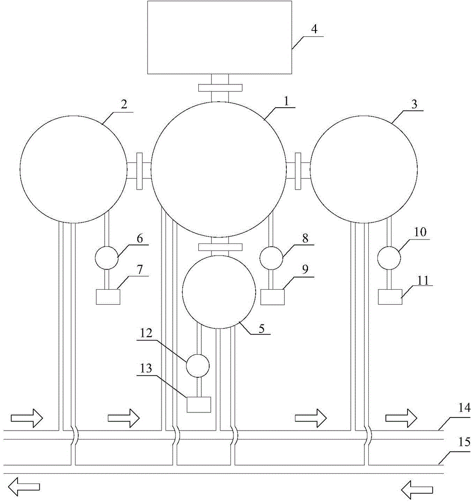
[0033] Such as figure 1 As shown, the optoelectronic device preparation system with online detection function provided in this embodiment includes a conversion chamber 1 , a first evaporation chamber 2 , a second evaporation chamber 3 , a glove box 4 and a detection chamber 5 . The conversion chamber 1 communicates with the first evaporation chamber 2 , the second evaporation chamber 3 , the glove box 4 and the detection chamber 5 respectively through a vacuum isolation valve.

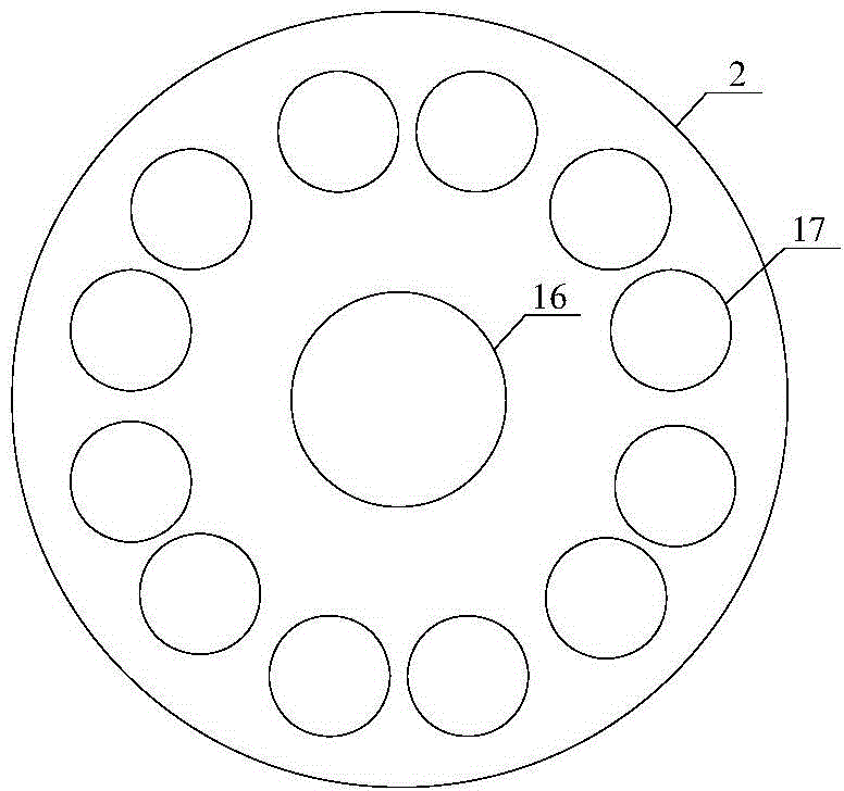
[0034] Such as figure 2 As shown, a first turntable 16 is set in the first evaporation chamber 2, and a plurality of organic material evaporation sources 17 are arranged around the first turntable 16, and the plurality of organic material evaporation sources 17 form a circle. In this embodiment, the number of organic material evaporation source...


PUM


Abstract

The invention discloses a photoelectric device manufacturing system with an online detection function. The photoelectric device manufacturing system comprises a conversion chamber (1), a first evaporation chamber (2), a second evaporation chamber (3), a glove box (4) and a detection chamber (5). The conversion chamber (1) is communicated with the first evaporation chamber (2), the second evaporation chamber (3), the glove box (4) and the detection chamber (5) through a vacuum isolation valve; a first rotary table (16) is arranged in the first evaporation chamber (2), and a plurality of organic material evaporation sources (17) are arranged on the periphery of the first rotary table (16); a second rotary table (18) is arranged in the second evaporation chamber (3), and a plurality of inorganic material evaporation sources (19) are arranged on the periphery of the second rotary table (18); the first rotary table (16) and the second rotary table (18) can rotate; a transmission device is arranged in the conversion chamber (1), and an online detection device is arranged in the detection chamber (5). According to the photoelectric device manufacturing system, online detection of performance of photoelectric devices can be achieved, and therefore the photoelectric devices can be prevented from being exposed to the atmospheric environment in the detection process.

Description

technical field [0001] The invention relates to the technical field of organic thin film preparation and organic photoelectric devices, in particular to a photoelectric device preparation system with on-line detection function. Background technique [0002] The rapid development of information science puts forward urgent requirements for information acquisition, transmission, storage, processing capacity and speed, making optoelectronics technology the most important technology field in the information field after microelectronics technology. Organic optoelectronics developed in recent years is an interdisciplinary subject of chemistry, information, materials and physics. It is a new technology developed by combining optical and electronic technologies. It is mainly used in the fields of information, energy and national defense. Organic optoelectronic functional materials and devices are playing an increasingly important role in the generation, transmission, storage and disp...

Claims


Application Information

Patent Timeline
Patent Type & Authority Applications(China)
IPC IPC(8): H01L51/00
CPCH10K71/00H10K71/70
Inventor 汪鹏飞孟令强张洪艳孟祥敏刘卫敏
Owner TECHNICAL INST OF PHYSICS & CHEMISTRY - CHINESE ACAD OF SCI
Why Eureka
Try Eureka