Supercharge Your Innovation With Domain-Expert AI Agents!

Metallic particle paste, cured product using same and semiconductor device

A technology of metal particles and cured products, which is applied in semiconductor devices, semiconductor/solid-state device manufacturing, semiconductor/solid-state device components, etc., and can solve problems such as the difficulty of pasting metal particles

Active Publication Date: 2015-03-18
KK TOSHIBA
View PDF6 Cites 10 Cited by
  • Summary
  • Abstract
  • Description
  • Claims
  • Application Information

AI Technical Summary

Problems solved by technology

[0007] However, since fine particles are usually aggregated to form secondary particles, it is very difficult to obtain a metal particle paste in which fine particles made of the first metal and fine particles made of the second metal are uniformly mixed

Method used


Image

  • Metallic particle paste, cured product using same and semiconductor device
  • Metallic particle paste, cured product using same and semiconductor device
  • Metallic particle paste, cured product using same and semiconductor device

Examples


Embodiment Construction

[0021] The metal particle paste according to the embodiment contains a polar solvent and particles containing a first metal dispersed in the polar solvent. A second metal different from the first metal is dissolved in the polar solvent.

[0022] Hereinafter, embodiments of the present invention will be described with reference to the drawings.

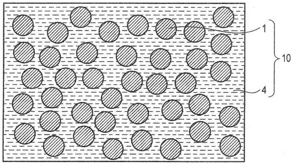
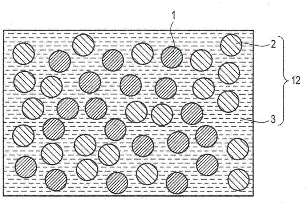
[0023] figure 1 It is a conceptual diagram of the metal particle paste concerning one embodiment. The metal particle paste 10 according to one embodiment contains two different metals, the first metal and the second metal. In the metal particle paste 10 of the present embodiment, the first metal is dispersed as the particles 1 in the polar solvent 4 , while the second metal is dissolved in the polar solvent 4 .

[0024] The metal particle paste of the present embodiment is cured to form a cured product in which the first metal mainly constitutes a mother phase responsible for electrical and thermal conductivity. As already explaine...


PUM

PropertyMeasurementUnit
particle diameteraaaaaaaaaa

Abstract

A metallic particle paste (10) includes a polar solvent (4) and particles (10) dispersed in the polar solvent and containing a first metal. A second metal different from the first metal is dissolved in the polar solvent. The second metal is present in solvent (10) of the metallic particle paste (10) in the form of a complex ion, an organometallic ion or an ion of a metal salt. The paste (10) may be used for forming wiring and a heat-radiation portion of an electronic substrate or for bonding members (5, 7) in a semiconductor device through a bonding layer (6).

Description

[0001] This application claims priority based on Japanese Patent Application No. 2013-187709 filed on September 10, 2013, the entire contents of which are incorporated herein by reference. technical field [0002] The embodiments described here generally relate to a metal particle paste, a cured product using the same, and a semiconductor device. Background technique [0003] Solder is used in electronic equipment as a material for bonding electronic parts and substrates, and has been becoming lead-free. However, in the case of solder applied to junctions of power devices that reach high temperatures during use, it is difficult to make lead-free. In recent years, wide bandgap semiconductors capable of operating at higher temperatures than Si have been developed, and the operating temperature of devices is predicted to reach about 300°C. Therefore, higher heat resistance is required for the joining material. [0004] At present, it is desired to improve the heat resistance ...

Claims


Application Information

Patent Timeline
Patent Type & Authority Applications(China)
IPC IPC(8): H01B1/22C09K5/10H01L23/29B22F1/054B22F1/107
CPCB23K35/0244H01L2224/05669H01L2224/83411H01L2224/05639H01L2224/2938H01L2224/83464H01L2224/325H01L2224/29371H01L2224/32507H01L24/32H01L2224/29324H01L24/05H01L2224/2732H01L2224/29355H01L2224/271H01L2224/32225H01L2924/1033H01L24/48H01L2224/83205H01L2924/10272H01L2224/05611H01L2224/29294H01L2224/04026H01L2224/2936H01L2224/83444B23K35/362H01L24/83H01L2224/42H01L2224/29364H01L2924/01102H01L2224/29376H01L2224/29313H01L2224/05655B23K35/24H01L2224/83439H01L2924/1067H01B1/22H01L2224/29344H01L2224/29318H01L2224/83203H01L2224/0381H01L2224/32245H01L2224/8384H01L2224/32503H01L2224/29347H01L2224/29373H01L2924/10254H01L2224/83455H01L2224/83192H01L2224/29369H01L2224/832H01L2224/29378H01L2224/29339H01L2224/2744H01L2224/27003H01L2224/2949H01L2224/05644H01L2224/83469H01L2224/83447H01L24/27H01L2224/8322H01B1/16H01L2224/29372H01L2224/05647H01L24/29B23K35/025H01L2924/10253H01L2224/83075H01L2224/2741H01L2224/05664B23K35/262B23K35/264B23K35/282B23K35/286B23K35/30B23K35/3006B23K35/3013B23K35/302B23K35/3033B23K35/32B23K35/322B23K35/325B23K35/3601H01L21/4867H01L23/3737B22F2999/00H01L2224/29006H01L2924/12044H01L2924/15787B22F1/107B22F1/054B22F1/09C22C1/047B22F1/0545H01L2924/0543H01L2924/01031H01L2924/00014H01L2924/00012H01L2924/00C22C5/06
Inventor 平塚大祐井口知洋内田雅之
Owner KK TOSHIBA
Features
  • R&D
  • Intellectual Property
  • Life Sciences
  • Materials
  • Tech Scout
  • Unparalleled Data Quality
  • Higher Quality Content
  • 60% Fewer Hallucinations
Learn More