SONOS (silicon oxide nitride oxide semiconductor) nonvolatile memory and manufacturing method thereof

A non-volatile, memory technology, used in semiconductor/solid-state device manufacturing, electrical solid-state devices, semiconductor devices, etc., to achieve the effect of reducing the area

Active Publication Date: 2015-03-18
SHANGHAI HUAHONG GRACE SEMICON MFG CORP
View PDF5 Cites 4 Cited by
  • Summary
  • Abstract
  • Description
  • Claims
  • Application Information

AI Technical Summary

Problems solved by technology

This further limits the shrinka

Method used


Image

  • SONOS (silicon oxide nitride oxide semiconductor) nonvolatile memory and manufacturing method thereof
  • SONOS (silicon oxide nitride oxide semiconductor) nonvolatile memory and manufacturing method thereof
  • SONOS (silicon oxide nitride oxide semiconductor) nonvolatile memory and manufacturing method thereof

Examples


Embodiment Construction

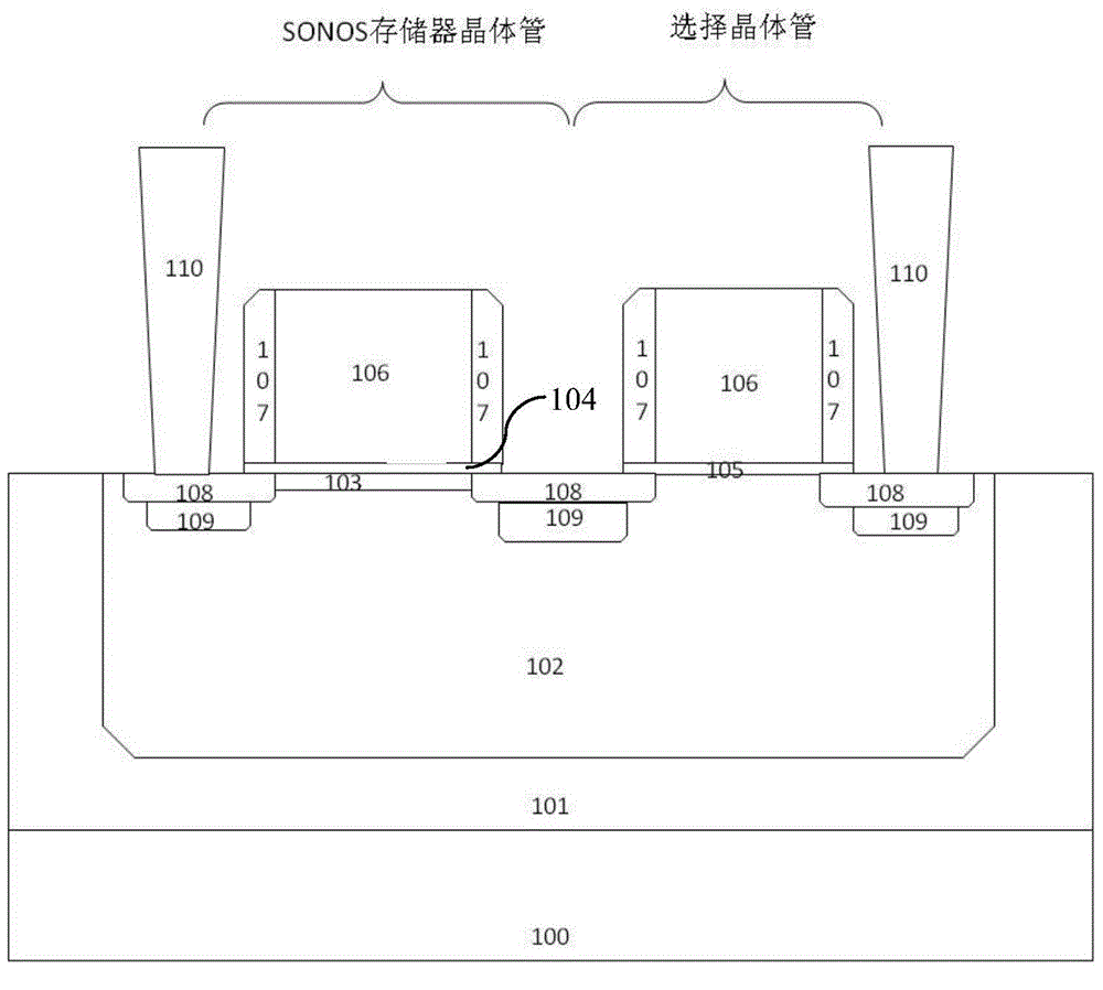
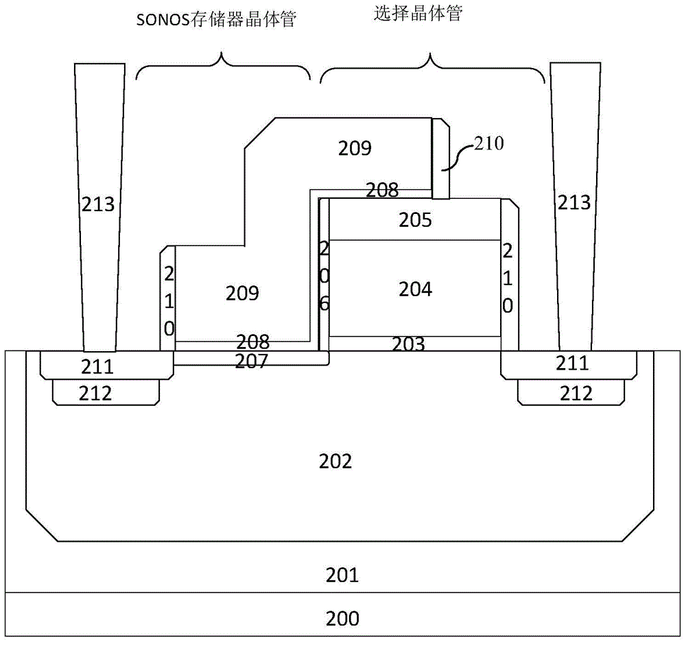
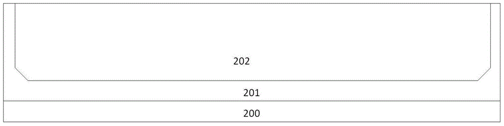
[0042] Such as figure 2 Shown is a cell structure diagram of the SONOS non-volatile memory of the embodiment of the present invention; the cell structure of the SONOS non-volatile memory of the embodiment of the present invention includes a SONOS memory transistor and a selection transistor, and the cell structure is formed in the P well 202 , the P well 202 is formed in the deep N well 201 of the silicon substrate 200 .

[0043] The gate structure of the SONOS memory transistor includes an ONO layer 208 and a first gate conductive material layer 209 sequentially formed on the surface of the P well 202. A three-layer structure composed of an oxide layer, a second nitride layer and a third oxide layer, the ONO layer 208 is used for charge storage; the surface part in the P well 202 at the bottom of the ONO layer 208 is formed with Tunnel implantation region 207, the tunnel implantation region 207 is used to provide electrons for direct tunneling, the tunnel implantation regio...


PUM


Abstract

The invention discloses a SONOS nonvolatile memory. A grid of a SONOS memory transistor and a grid of a selective transistor of a unit structure of the SONOS nonvolatile memory are of a two-layer isolated overlapped structure; the first side face of the selective transistor is provided with a first insulating medium side wall; a tunnel injection region and an ONO layer of the SONOS memory transistor are aligned with the first insulating medium side wall; the whole unit structure only comprises two source and drain regions; no source and drain regions exist between the grid of the SONOS memory transistor and the selective transistor. The invention also discloses a method for manufacturing the SONOS nonvolatile memory. A source and drain region between grids of the two transistors is omitted directly, the area of the memory unit can be greatly reduced, and an additional etching step is not added.

Description

technical field [0001] The invention relates to a semiconductor integrated circuit manufacturing process method, in particular to one. Background technique [0002] SONOS non-volatile memory is widely used in advanced flash memory and electrically erasable memory products. At present, the commonly used memory cell structure consists of a complete SONOS memory transistor and a complete select transistor to form a 2-transistor structure (2T structure), each transistor has a complete source, drain and gate, and the two transistors share a layer polysilicon. Such as figure 1 Shown is the cell structure diagram of the existing SONOS non-volatile memory; the cell structure of the existing SONOS non-volatile memory includes a SONOS memory transistor and a selection transistor, the cell structure is formed in the P well 102, the P Well 102 is formed in deep N-well 101 of silicon substrate 100 . [0003] The gate structure of the SONOS memory transistor includes an ONO layer 104 ...

Claims


Application Information

Patent Timeline
IPC IPC(8): H01L27/115H01L21/8247
Inventor 陈瑜袁苑陈华伦
Owner SHANGHAI HUAHONG GRACE SEMICON MFG CORP
Why Eureka
Try Eureka