Optical fiber and silicon waveguide coupling structure based on polymer waveguides and manufacturing method thereof

A coupling structure and polymer technology, applied in the coupling of optical waveguide, light guide, optics, etc., can solve the problems of complex process and low reliability of optical fiber coupling structure, reduce process complexity, ensure reliability, and improve coupling efficiency Effect

Active Publication Date: 2015-03-25
WUHAN POST & TELECOMM RES INST CO LTD
View PDF4 Cites 17 Cited by
  • Summary
  • Abstract
  • Description
  • Claims
  • Application Information

AI Technical Summary

Problems solved by technology

[0004] The technical problem to be solved by the present invention is the problem of complex process and low reliability of the optical fiber coupling structure

Method used


Image

  • Optical fiber and silicon waveguide coupling structure based on polymer waveguides and manufacturing method thereof
  • Optical fiber and silicon waveguide coupling structure based on polymer waveguides and manufacturing method thereof
  • Optical fiber and silicon waveguide coupling structure based on polymer waveguides and manufacturing method thereof

Examples


Embodiment Construction

[0024] The present invention will be described in detail below in conjunction with the accompanying drawings and specific embodiments.

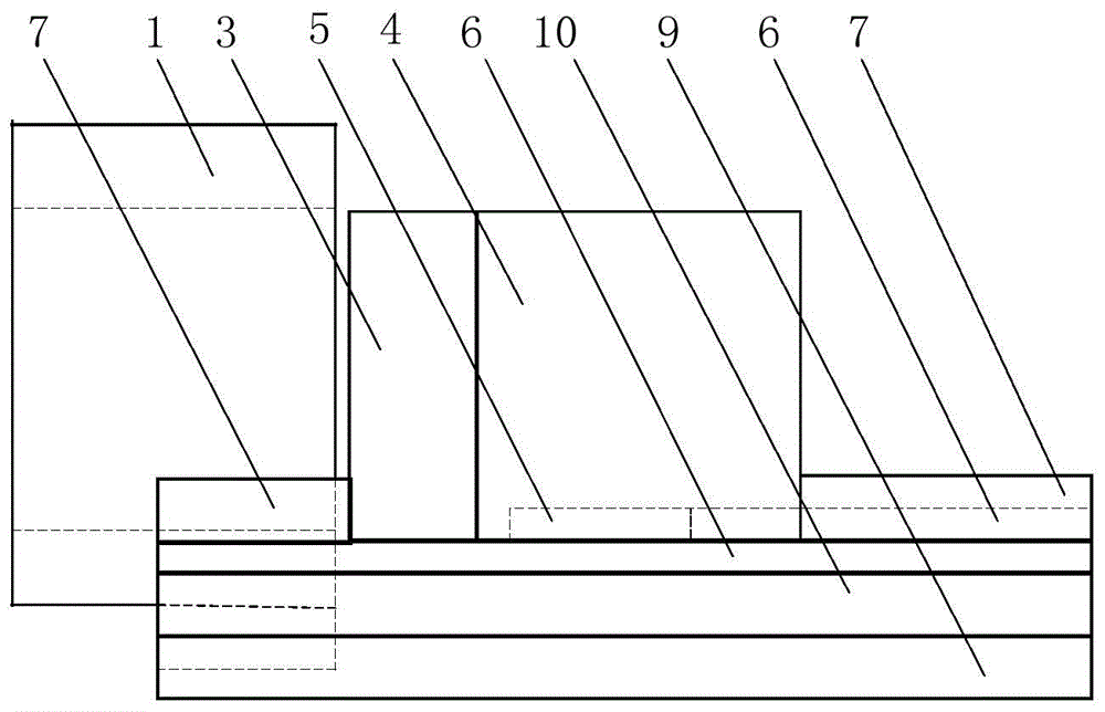
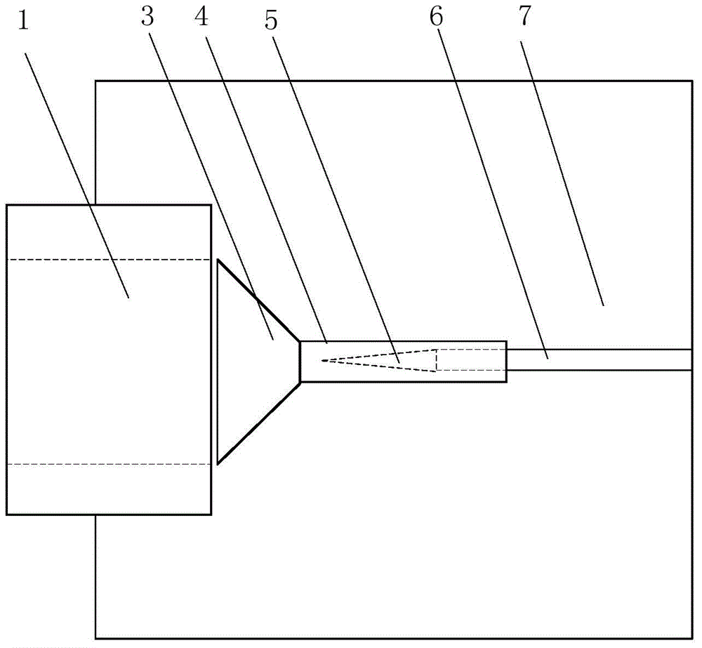
[0025] Such as figure 1 , 2 As shown in 3 and 3, the optical fiber and silicon waveguide coupling structure based on polymer waveguide provided by the present invention includes an SOI (Silicon-On-Insulator, silicon-on-insulator) wafer and an optical fiber 1 disposed on the SOI wafer.

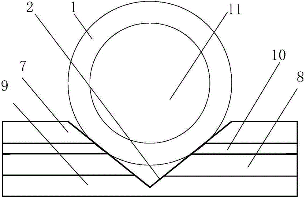
[0026] The SOI wafer includes an upper layer silicon 10, a buried oxide layer 8 and a substrate silicon 9 from top to bottom;

[0027] The upper layer of silicon 10 is provided with polymer straight waveguides 4 and polymer tapered waveguides 3 arranged in sequence from right to left, and the part of the upper layer of silicon 10 where the polymer straight waveguides and polymer tapered waveguides are not arranged is covered with a layer of silicon dioxide. Layer 7, the narrow end of the polymer tapered waveguide 3 is connected to the polymer straight wavegu...


PUM


Abstract

The invention discloses an optical fiber and silicon waveguide coupling structure based on polymer waveguides and a manufacturing method of the optical fiber and silicon waveguide coupling structure. The optical fiber and silicon waveguide coupling structure based on the polymer waveguides comprises an SOI wafer and an optical fiber arranged on the SOI wafer, the polymer straight waveguide and the polymer tapered waveguide are arranged on a buried oxide layer of the SOI wafer in sequence from right to left, the narrower end of the polymer tapered waveguide is connected with the polymer straight waveguide, and the wider end of the polymer tapered waveguide is aligned with a fiber core of the optical fiber; the silicon waveguide is arranged on upper layer silicon, the left end of the silicon waveguide is a back taper structure with a gradually changing width, the right end of the silicon waveguide is of a straight silicon waveguide back taper structure, part of the straight silicon waveguide wrapped in the polymer straight waveguide, and other parts of the straight silicon waveguide is covered with a silicon dioxide covering layer; a V-shaped groove is formed in the top surface of the left end of the SOI wafer, the silicon dioxide covering layer, the upper layer silicon and the buried oxide layer sequentially penetrate through the V-shaped groove in the depth direction, and the bottom end of the V-shaped groove is located at substrate silicon; the optical fiber is fixed in the V-shaped groove. The optical fiber and silicon waveguide coupling structure based on the polymer waveguides and the manufacturing method of the optical fiber and silicon waveguide coupling structure not only improve coupling efficiency, reduce process complexity and guarantee the reliability of the optical fiber coupling structure.

Description

technical field [0001] The invention relates to the field of optical communication devices, in particular to an optical fiber and silicon waveguide coupling structure based on a polymer waveguide and a manufacturing method thereof. Background technique [0002] Fiber coupling is an important technology in the packaging of optical integrated devices. Small waveguide cross-sections are often used, which can make high-refractive index waveguide devices very compact. However, the huge mode mismatch between the fiber and the high-index waveguide in this scheme will lead to high coupling loss. For this reason, the existing technology uses an inverted tapered coupler to solve the problem of mode mismatch between the optical fiber and the high-refractive index waveguide. The principle is: firstly, the light is coupled from the optical fiber to a low-refractive-index waveguide; Inverted cone coupler. [0003] At present, the inverted cone coupler coupled with the planar optical fib...

Claims


Application Information

Patent Timeline
Patent Type & Authority Applications(China)
IPC IPC(8): G02B6/26
CPCG02B6/264
Inventor 王磊
Owner WUHAN POST & TELECOMM RES INST CO LTD
Why Eureka
Try Eureka