
Preparation method for LED perpendicular structure

A technology of vertical structure and LED epitaxial wafer, which is applied in semiconductor/solid-state device manufacturing, electrical components, circuits, etc. It can solve the problems of GaN surface treatment difficulties, increased loss of thin film defects, and restrictions on large-scale applications, and achieve low cost and high-quality devices. Efficiency improvement, simple and reliable method

Inactive Publication Date: 2015-03-25
西安利科光电科技有限公司
View PDF5 Cites 9 Cited by
  • Summary
  • Abstract
  • Description
  • Claims
  • Application Information

AI Technical Summary

Problems solved by technology

Although laser lift-off technology has become a new research hotspot due to its high efficiency and low damage, there are also some shortcomings that limit large-scale applications, specifically: low yield, high cost, not suitable for large-size substrates, and high precision requirements. lead to the increase of defect loss in the film, and the metallic Ga part generated by laser irradiation combines with the oxygen in the air to form Ga 2 o 3 , making it difficult to post-treat the GaN surface after stripping

Method used


Image

  • Preparation method for LED perpendicular structure
  • Preparation method for LED perpendicular structure
  • Preparation method for LED perpendicular structure

Examples


Embodiment Construction

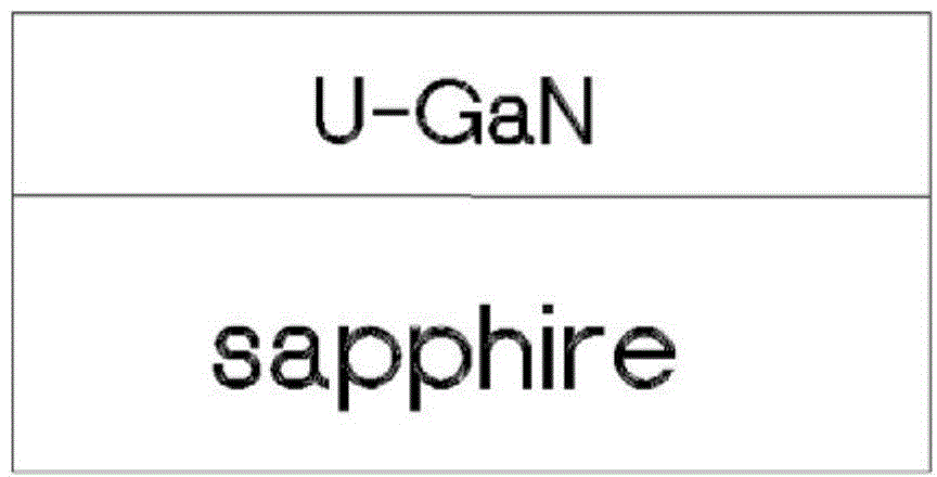
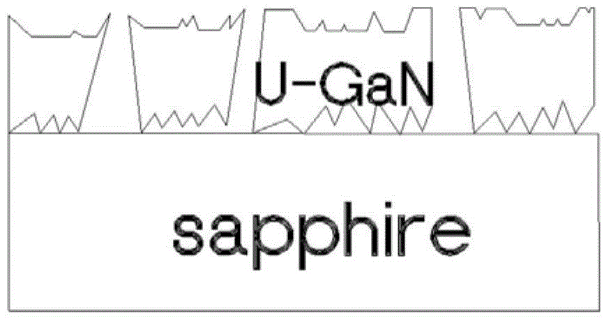
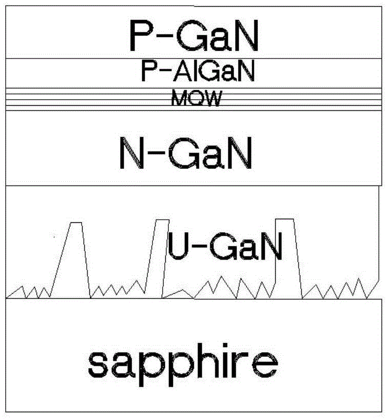
[0038] The main feature of the present invention is: after U-GaN grows, carry out wet etching (KOH or H 3 PO 4Wet etching); etch through GaN defects (GaN growth on a heterogeneous substrate (sapphire) itself will generate a large number of defects) to the GaN / sapphire interface, and etch in both directions, followed by The wafer enters the epitaxial equipment again for GaN epitaxial growth, and the regrown GaN will directly grow GaN on the etched GaN instead of on the sapphire. In this way, part of the stress of GaN is released, and this process will leave an inverted pyramid structure at the GaN at the sapphire interface, so that a point contact is formed between GaN and sapphire, which is conducive to the subsequent peeling of the epitaxial layer to form a vertical structure. Prepare a reflector (Ti / Ni / Ag or Ti / Ni / Al) on the surface of the P-GaN epitaxial layer; finally, use a high-temperature metal bonding process to bond the P-GaN (electrode) to a silicon or copper or tun...


PUM


Abstract

The invention relates to a preparation method for an LED perpendicular structure. With a substrate or a substrate with a low-temperature GaN buffer layer as the growth foundation, U-GaN and all other layers of epitaxy sequentially grow, and the growth of an LED epitaxial wafer is completed. The method includes the steps of firstly, conducting wet etching till the surface of the growth foundation after the growth of the U-GaN layer is completed; secondly, continuing to grow U-GaN, and then sequentially growing the other layers of epitaxy on the surface of the U-GaN so as to obtain the LED epitaxial wafer, wherein the new U-GaN can directly grow on the etched U-GaN, and an inverted pyramid structure is left on the U-GaN on the surface of the growth foundation; thirdly, obtaining the LED perpendicular structure through the LED epitaxial wafer, wherein deposition is conducted on the surface of the LED epitaxial wafer to form a reflection mirror, one metal electrode pattern is manufactured, the surface of the metal electrode pattern is bonded on a metal base plate through the high-temperature metal bonding process, the substrate is stripped through the normal-temperature ultrasonic technology, and the other metal electrode pattern is manufactured on the surface of the U-GaN. By means of the preparation method, cost can be effectively reduced, and efficiency can be effectively improved.

Description

Technical field: [0001] The invention belongs to the preparation technology of semiconductor devices, and in particular relates to a preparation method of an LED vertical structure. Background technique: [0002] At present, the world has entered the "energy-saving era", and all countries are actively looking for new energy-saving and environmentally friendly industries. The energy consumed by lighting accounts for more than 20% of the total energy consumption. Therefore, reducing lighting power consumption is an important way to save electricity. LED energy-saving lamp is a new generation of solid-state cold light source, which has the characteristics of low energy consumption, long life, easy control, safety and environmental protection, etc. It is an ideal energy-saving and environmental protection product, suitable for various lighting places. However, at present, LEDs have not entered general lighting on a large scale. One of the main reasons is that the cost performanc...

Claims


Application Information

Patent Timeline
Patent Type & Authority Applications(China)
IPC IPC(8): H01L33/00H01L21/683H01L33/22
CPCH01L33/005H01L21/68757H01L33/22H01L33/62H01L2933/0008H01L2933/0033
Inventor 胡丹宁磊缪炳有黄宏嘉
Owner 西安利科光电科技有限公司
Learn More