Preparation method for low-cost GaN-based light emitting diode

A light-emitting diode, gallium nitride-based technology, applied in electrical components, circuits, semiconductor devices, etc., can solve problems such as being unsuitable for high current density conditions, and achieve the effects of avoiding current blocking effects, reducing manufacturing costs, and improving luminous efficiency.

Active Publication Date: 2015-03-25
TAIYUAN UNIV OF TECH
View PDF1 Cites 4 Cited by
  • Summary
  • Abstract
  • Description
  • Claims
  • Application Information

AI Technical Summary

Problems solved by technology

However, the disadvantage of this method is that an AlN layer needs to be inserted between the boron nitride and the LED epitaxial structure to improve the surface morphology of the LED.
The insertion la

Method used


Image

  • Preparation method for low-cost GaN-based light emitting diode

Examples


Embodiment 1

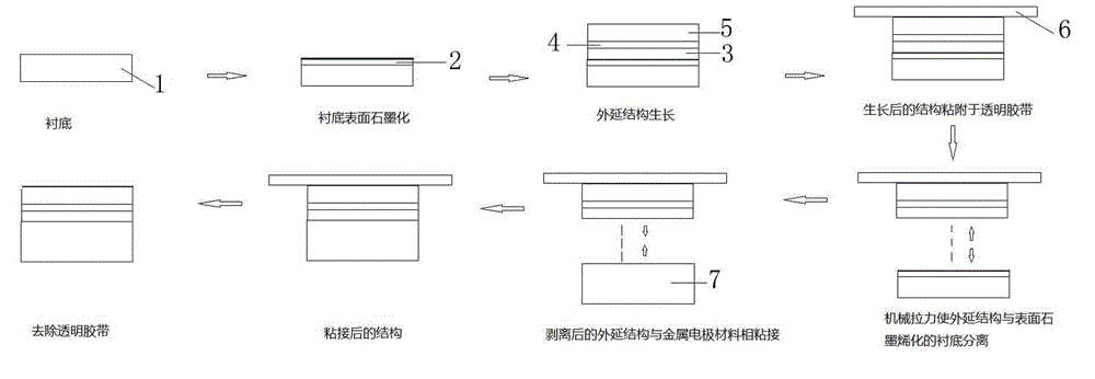
[0021] The preparation method of LED structure described in embodiment 1, concrete steps are as follows:

[0022] 1) When the reaction temperature of the crystalline flake TiC material reaches 850°C, the reaction temperature is kept at 850°C for 15 minutes to realize the detitanium removal process on the surface, then the chlorine gas source is turned off, and argon gas is passed in, and the temperature is still maintained at 850°C for 20 minutes to achieve Grapheneization of the surface layer, the number of graphene layers is 6 layers, and the graphene is in the form of undulating wrinkled surfaces, with a height difference within 15nm; the thickness of the thin-sheet TiC substrate can be selected from 300um to 1mm;

[0023] 2) Put the flaky TiC substrate 1 material whose surface has been grapheneized into the MOCVD reaction chamber to sequentially grow the n-type doped layer, the multi-quantum well light-emitting layer and the p-type doped layer epitaxial structure. The grow...

Embodiment 2

[0028] The preparation method of LED structure described in embodiment 2, concrete steps are as follows:

[0029] 1) When the reaction temperature of amorphous TiC flakes reaches 500 °C, chlorine gas is passed in for 10 minutes to realize the detitanium removal process on the surface, then the chlorine gas source is turned off, argon gas is introduced, and the temperature is raised to 850 °C to keep 15 minutes to realize the grapheneization of the surface layer; the number of graphene layers is 3 layers, and the graphene is in the shape of undulating wrinkled surfaces, and the height difference of the fluctuations is within the range of 10nm; the thickness of the flake TiC substrate can be selected from 300um to 1mm;

[0030]2) Put the flaky TiC substrate 1 material whose surface has been grapheneized into the MOCVD reaction chamber to sequentially grow the n-type doped layer, the multi-quantum well light-emitting layer and the p-type doped layer epitaxial structure. The growt...


PUM

PropertyMeasurementUnit
Thicknessaaaaaaaaaa
Thicknessaaaaaaaaaa

Abstract

The invention relates to a preparation method for a low-cost GaN-based light emitting diode. The preparation method for the low-cost GaN-based light emitting diode aims to solve the technical problems that existing light emitting diode preparation methods are high in cost, and substrates can hardly be utilized repeatedly. The preparation method for the low-cost GaN-based light emitting diode comprises the steps that a lamelliform TiC material with the surface covered with graphene serves as a substrate material, a light emitting diode epitaxial structure grows on the substrate material, and the epitaxial structure comprises an n-type doping layer, a multiple-quantum-well light emitting layer and a p-type doping layer. According to the preparation method for the low-cost GaN-based light emitting diode, the lamelliform TiC material with the surface covered with graphene serves as the substrate material, separation of the substrate and the epitaxial structure is achieved through weak Van der Waals' force between the graphene and the epitaxial layer and mechanical tensile force, repeated using of the substrate is achieved, and the manufacturing cost of devices is lowered.

Description

technical field [0001] The invention relates to a preparation method of a gallium nitride-based light-emitting diode, and more particularly relates to a preparation method of a low-cost gallium nitride-based light-emitting diode with reusable substrate materials. Background technique [0002] After years of development of light-emitting diodes, the light efficiency has been significantly improved. However, one of the key problems restricting its widespread application is that it is still at a disadvantage compared with ordinary energy-saving lamps and incandescent lamps in terms of cost. The traditional preparation method of gallium nitride-based light-emitting diodes uses expensive SiC or sapphire wafers as substrate materials, and the substrate materials can only be used once. IBM proposed a method of grapheneizing the surface of SiC to re-grow GaN-based light-emitting epitaxial structures. After the growth is completed, the entire GaN film is transferred to the silicon s...

Claims


Application Information

Patent Timeline
IPC IPC(8): H01L33/16H01L33/00
CPCH01L33/0075H01L33/14H01L33/16H01L2933/0008
Inventor 李天保贾伟许并社梁建余春艳章海霞
Owner TAIYUAN UNIV OF TECH
Why Eureka
Try Eureka