Flip eutectic LED packaging method
A technology of LED packaging and LED chips, applied in electrical components, circuits, semiconductor devices, etc., can solve the problems of high product restrictions, unsuitable use, short mold life, etc., to improve production efficiency and quality, and promote the welding process. , the effect of reducing costs
- Summary
- Abstract
- Description
- Claims
- Application Information
AI Technical Summary
Problems solved by technology
Method used
Image
Examples
Embodiment 1
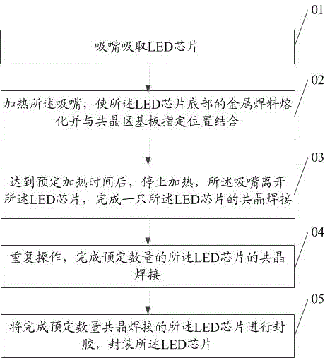
[0038] This embodiment provides a flip-chip eutectic LED packaging method, such as figure 1 shown, including the following steps:
[0039] 01. The suction nozzle sucks the LED chip.
[0040] 02. Heat the suction nozzle to melt the metal solder at the bottom of the LED chip and combine it with the specified position of the eutectic region substrate. The substrate may be a ceramic substrate, a copper substrate, an aluminum substrate, or the like. It is possible, but not limited to, to heat the suction nozzle using pulse heating.
[0041] It may be, but not limited to, after the suction nozzle picks up the LED chip and before combining it with the specified position of the eutectic region substrate, it may also include sticking appropriate flux on the LED chip in a flux box.
[0042] 03. After the predetermined heating time is reached, the heating is stopped, the suction nozzle leaves the LED chip, and the eutectic welding of one LED chip is completed.
[0043] 04. Repeat the...
Embodiment 2
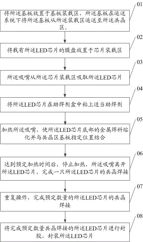
[0056] The difference between this embodiment and embodiment 1 is that, as image 3 As shown, before the suction nozzle picks up the LED chips, it also includes:
[0057] 01. The substrate is placed in the substrate loading area, and the substrate is transported from the loading area to the eutectic area under the transport system.
[0058] It can be but not limited to, before the suction nozzle picks up the LED chip, it also includes:
[0059] 02. Place the film disc carrying the LED chip in the chip loading area,
[0060] 03. The suction nozzle sucks the LED chip from the chip loading area.
[0061] 04. Paste appropriate flux on the LED chip in the flux box.
[0062] 05. Heat the suction nozzle to melt the metal solder at the bottom of the LED chip and combine it with the designated position of the eutectic region substrate. The substrate may be a ceramic substrate, a copper substrate, an aluminum substrate, or the like. It is possible, but not limited to, to heat the s...
Embodiment 3
[0070] In this embodiment, a ceramic material substrate is used, and the LED chip whose bottom is gold-tin alloy (Au:Sn=80%:20%) is used.
[0071] The ceramic substrate and the LED chip are respectively placed on the substrate loading area and the chip loading area, and the LED chip is picked up by using a suction nozzle, and the soldering flux is pasted on it. The pulse heating system starts to heat the suction nozzle, and after the temperature reaches the melting point of metal solder (282°C), the LED chip is placed on the ceramic substrate that has been transferred from the loading area to the eutectic area, and it stays for 0.5 Seconds later, stop heating the suction nozzle, and at the same time, the suction nozzle leaves the LED chip to complete the eutectic of one LED chip.
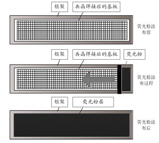
[0072] Place the ceramic substrate after several LED chip eutectics have been completed on a flat table, fix a frame 0.05mm higher than the LED chip around the ceramic substrate, and place the glue ...
PUM
 Abstract
Description
Claims
Application Information
 - R&D
- Intellectual Property
- Life Sciences
- Materials
- Tech Scout
- Unparalleled Data Quality
- Higher Quality Content
- 60% Fewer Hallucinations
Browse by: Latest US Patents, China's latest patents, Technical Efficacy Thesaurus, Application Domain, Technology Topic, Popular Technical Reports.
© 2025 PatSnap. All rights reserved.Legal|Privacy policy|Modern Slavery Act Transparency Statement|Sitemap|About US| Contact US: help@patsnap.com


