Circuit board debugging and detecting system and application method thereof

A detection system and circuit board technology, applied in the direction of electronic circuit testing, etc., can solve problems such as low accuracy, error-prone, and many hidden dangers, and achieve the effects of eliminating the cause of failure, facilitating management, and improving detection efficiency

Inactive Publication Date: 2015-04-08
NO 60 RES INST OF GENERAL STAFF DEPT PLA
View PDF5 Cites 3 Cited by
  • Summary
  • Abstract
  • Description
  • Claims
  • Application Information

AI Technical Summary

Problems solved by technology

[0003] The long production cycle of the circuit board will affect the debugging progress and delivery time of the whole machine, but it takes a lot of time to debug and detect the circuit board to eliminate hidden dangers in the production of the circuit board; the current circuit board debugging and testing are mainly through the cable The plug-in is connected to each interface of the circuit board, which has low efficiency, many hidden dangers, and the quality cannot be guaranteed. It also lacks the detection data analysis and statis

Method used


Image

  • Circuit board debugging and detecting system and application method thereof
  • Circuit board debugging and detecting system and application method thereof
  • Circuit board debugging and detecting system and application method thereof

Examples


Example Embodiment

[0030] Example 1

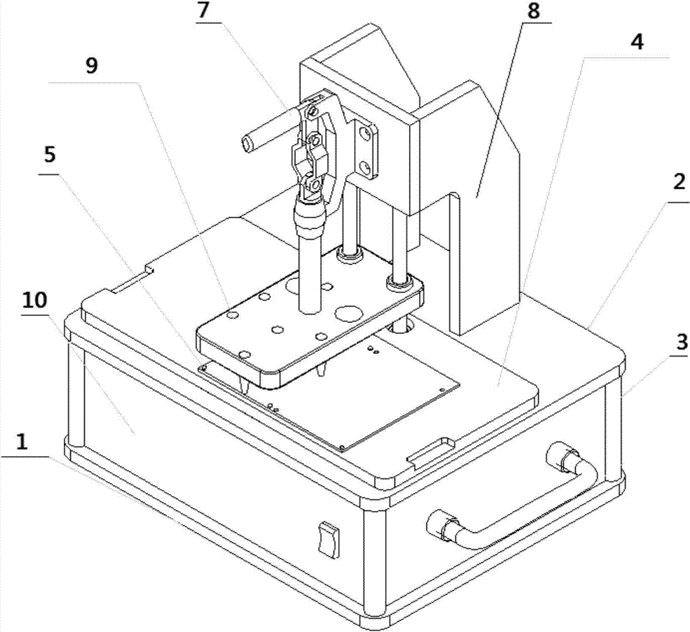
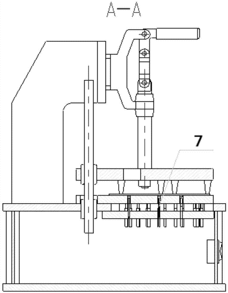
[0031] like Figure 1 to Figure 3 As shown, a circuit board debugging and testing system provided in this embodiment includes a probe fixture and a transmission system built in the probe fixture and a PC respectively, wherein: the probe fixture includes a square bottom plate arranged horizontally And the square panel located above the bottom plate, the bottom plate and the panel are corresponding and parallel to each other, the bottom plate and the panel are fixedly connected by aluminum support columns vertically arranged at the four corners, and the panel is also laid with a PCB supporting board. The PCB supporting plate is installed on the panel through springs, limit screws and bearing columns. There is also a detection slot in the middle of the PCB supporting plate for placing the circuit board to be tested, and a probe is provided on the upper surface of the detection slot;

[0032] It also includes a support frame vertically arranged on the panel, ...

Example Embodiment

[0037] Example 2

[0038] like Figure 4 As shown, the application method of a circuit board debugging and detection system provided in this embodiment includes the following specific steps:

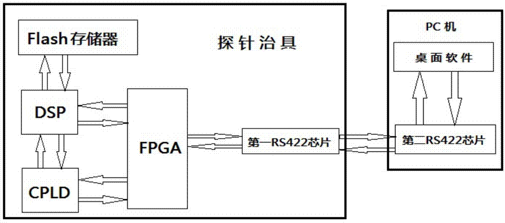
[0039] Step (1) First use FPGA to determine the receiving timing and sending timing of running DSP for serial port debugging, and use DSP for serial port debugging;

[0040] Step (2) Place the circuit board to be tested, quickly clamp the circuit board with the clamp, and connect each test point through the probe. The desktop software analyzes, records and counts the data while testing the circuit board.

[0041] Furthermore, in the application method of the aforementioned circuit board debugging and detection system, the specific operation of step (1) is as follows:

[0042] Step a: correspondingly connect the sending pin of the first RS422 serial chip set with the receiving pin of the second RS422 serial chip set;

[0043] Step b: connect the JTAG port of CPLD, and download it;

...


PUM


Abstract

The invention discloses a circuit board debugging and detecting system and an application method thereof. The circuit board debugging and detecting system comprises a probe fixture and transmission systems embedded in the probe fixture and a PC (personal computer) respectively. The application method of the circuit board debugging and detecting system adopts a probe connection way and is accurate in positioning, various test ports of circuits can be quickly connected, and operation time is greatly saved. The invention further provides a data analysis and processing desktop software system capable of tracking and recording in the whole process of detection of the circuit boards, various ports of the circuit boards can be detected, in the meantime, data are acquired and analyzed, so that fault points and reasons are outputted; detecting results of batches can be counted, yield rate of the batches and fault distribution of the circuit boards are outputted, devices of the circuit boards are welded and effectively monitored, detection efficiency of the circuit boards is improved, management of welding quality of the circuit boards in the batches and elimination of the fault reasons are facilitated.

Description

technical field [0001] The invention relates to the technical field of process debugging, which collects and analyzes data through quick connection of probes and software, in particular to a circuit board debugging and detection system and an application method thereof. Background technique [0002] With the advancement of science and technology, the development of the electronics industry is advancing by leaps and bounds, the electronic system is becoming more and more complex, and the reliability and maintainability requirements of the electronic system are also getting higher and higher. As the control unit of various terminals and components, the circuit board is the product function The core of the implementation, its quality directly affects the quality of the entire device. [0003] The long production cycle of the circuit board will affect the debugging progress and delivery time of the whole machine, but it takes a lot of time to debug and detect the circuit board t...

Claims


Application Information

Patent Timeline
IPC IPC(8): G01R31/28
Inventor 张剑飞严华化汤捷何剑明石小红崔巍庄震宇
Owner NO 60 RES INST OF GENERAL STAFF DEPT PLA
Why Eureka
Try Eureka