A method for rapidly completing the operation of chip buckling edge sheet, a mold, a mold manufacturing method, and a mold storage device

A manufacturing method and edge-cutting technology, which are applied in semiconductor/solid-state device manufacturing, electrical components, circuits, etc., can solve problems such as low production efficiency and cumbersome operation, and achieve the effects of improved efficiency, high economic benefits, and high flatness

Active Publication Date: 2017-07-07
马鞍山太时芯光科技有限公司
View PDF2 Cites 0 Cited by
  • Summary
  • Abstract
  • Description
  • Claims
  • Application Information

AI Technical Summary

Problems solved by technology

[0005] Aiming at the problems of time-consuming, cumbersome operation and low production efficiency in the existing LED chip edge-cutting operation, the present invention provides a method for quickly completing the chip-cutting edge piece operation, a mold, a mold manufacturing method and a mold storage device. When the invented mold is used for chip buckling operation, it does not need to be heated by a heating machine, and the side piece can be quickly poured into the finished film by simply pressing the blue film above the chip side piece to complete the chip side buckle operation

Method used


Image

  • A method for rapidly completing the operation of chip buckling edge sheet, a mold, a mold manufacturing method, and a mold storage device
  • A method for rapidly completing the operation of chip buckling edge sheet, a mold, a mold manufacturing method, and a mold storage device
  • A method for rapidly completing the operation of chip buckling edge sheet, a mold, a mold manufacturing method, and a mold storage device

Examples


Embodiment 1

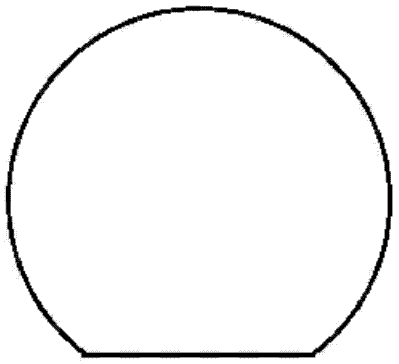
[0045] Such as figure 1 As shown in the figure, a mold for quickly completing the operation of buckling the edge of the chip, the mold is in the shape of a disc, with a diameter of D = 78-[x] / 2mm, where x is the percentage value of the edge in the photoelectric parameter diagram of the chip, [x] Indicates that x is rounded to a single digit according to the rounding principle (the side part of the chip is a chip with poor photoelectric parameters, in order to ensure that the center part of the chip is not mixed with chips with poor photoelectric parameters, the Appropriately relax the ratio to improve the quality of the center chip. Therefore, in the actual production process of the enterprise, when [x] is 6-10, press [x] to be 13 to make a mold of the corresponding size, and when [x] is 11-15, press [x] is 18 to make the mold of corresponding size, and [x] is 16-20 to be 23 to make the mold of corresponding size by [x], the mold of preparation 3 sizes gets final product.), in...

Embodiment 2

[0063] A mold for quickly completing the operation of buckling the edge of the chip. The mold is in the shape of a disc, with a diameter of D=78-[x] / 2mm, where x is the percentage value of the edge in the photoelectric parameter diagram of the chip, and [x] represents the basis of rounding In principle, x is rounded to a single digit. In this example, [x] is 13. In the actual production process, [x] is 18 to make a mold of the corresponding size. The mold is made of blue film and flat release paper , There is a slit on the edge of the mold, the distance between the slit and the center of the mold is 2 / 15 of the diameter of the mold, and the thickness of the mold is 2mm.

[0064] The preparation steps of the blue film in this example are as follows: heating and melting the polybutylene terephthalate (polyester) raw material, and then using a PET transparent film (thickness of 100 μm) as the base layer, and using a flat film scraping machine on its surface (Denoted as A side) sc...

Embodiment 3

[0081]A mold for quickly completing the operation of buckling the edge of the chip. The mold is in the shape of a disc, with a diameter of D=78-[x] / 2mm, where x is the percentage value of the edge in the photoelectric parameter diagram of the chip, and [x] represents the basis of rounding In principle, x is rounded to a single digit. In this example, [x] is 20. In the actual production process, [x] is 23 to make a mold of the corresponding size. The mold is made of blue film and flat release paper , There is a slit on the edge of the mold, the distance between the slit and the center of the mold is 1 / 8 of the diameter of the mold, and the thickness of the mold is 1.5mm.

[0082] The preparation steps of the blue film in this example are as follows: heating and melting the polybutylene terephthalate (polyester) raw material, and then using a PET transparent film (thickness of 300 μm) as the base layer, and using a flat film scraping machine on its surface (Denoted as A side) sc...


PUM

PropertyMeasurementUnit
diameteraaaaaaaaaa
thicknessaaaaaaaaaa
peel strengthaaaaaaaaaa

Abstract

The invention discloses a method and a mold for rapidly finishing chip edge sheet buckling operation, a mold manufacturing method and a mold storing device, and belongs to the field of semiconductor devices. The mold is a wafer of which the diameter D=78-[x] / 2mm ([x] is an integer between 6 and 20); a blue film and planar release paper are taken as manufacturing materials; the edge of the mold is provided with a notch. The mold disclosed by the invention is simple in structure, is reasonable in design, is easy to manufacture, and has an unexpected use effect. By adopting the mold, the batch edge buckling operation of a chip can be realized. Compared with the conventional complex edge-buckling method, the method disclosed by the invention has the advantages that the efficiency is increased by 70-80 percent, a good edge-buckling effect is achieved, the edge of the edge-buckled chip is flush, the chip is free from damage, and the cost is low.

Description

technical field [0001] The invention belongs to the field of semiconductor device manufacturing, and more specifically, relates to a method for rapidly completing the operation of chip buckling, a mold, a mold manufacturing method, and a mold storage device. Background technique [0002] With the advent of light-emitting diodes (LEDs) in 1960, LEDs began to be widely used in our surroundings, playing a pivotal role in daily life, and becoming one of the most valued light source technologies, such as various indicator lights , display light source and lighting equipment, etc. can see the application of LED. Compared with traditional lighting sources such as fluorescent lamps and incandescent tungsten bulbs, LEDs have the advantages of high brightness, low power consumption, long life, fast startup, small size, environmental protection and energy saving, and are not prone to visual fatigue. They have broad development prospects. , has received widespread attention. The manuf...

Claims


Application Information

Patent Timeline
Patent Type & Authority Patents(China)
IPC IPC(8): H01L21/67H01L33/48
CPCH01L21/67011H01L33/48
Inventor 朱燕李有群许静廉鹏
Owner 马鞍山太时芯光科技有限公司
Why Eureka
Try Eureka