

Method for manufacturing binary optical element with transparent ceramic as substrate material
A binary optical element and transparent ceramic technology, applied in the field of optical materials, can solve the problems of low hardness, high brittleness and opacity, and achieve the effect of low hardness and high brittleness
- Summary
- Abstract
- Description
- Claims
- Application Information
AI Technical Summary
Problems solved by technology
Method used
Image

Examples
Embodiment 1
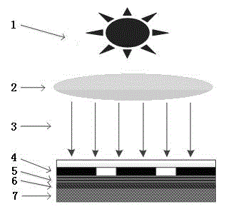
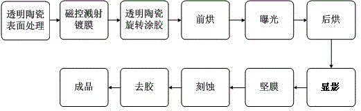
[0041] The invention discloses a method for making a binary optical element using transparent ceramics as a base material. Undoped yttrium aluminum garnet transparent ceramics are used as the base material of the binary optical element. The process flow includes: transparent ceramic surface treatment, magnetron control Sputtering coating, spin coating, pre-baking, exposure, post-baking, developing, hardening, etching and degumming processes.
[0042] 1) Transparent ceramic surface treatment
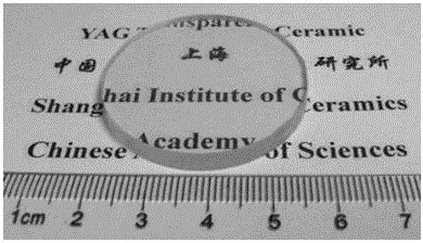
[0043] The transparent ceramics (YAG for short) are pre-coated, polished by a grinder to obtain transparent ceramics with a surface close to the mirror surface, cleaned with an alcohol solution, and then cleaned with an ultrasonic cleaner for 5 minutes. After the ceramic surface is completely dry, it enters the coating stage.
[0044] 2) Magnetron sputtering anti-oxidation metal film
[0045] 2.1 Clean the magnetron sputtering furnace cavity with alcohol to remove dirt, attachments a...
PUM
 Abstract
Description
Claims
Application Information