Silicon carbide ohmic contact electrode and manufacturing method of silicon carbide ohmic contact electrode

A technology of ohmic contact electrode and ohmic contact, which is applied in the direction of circuits, electrical components, semiconductor devices, etc., and can solve problems such as corrosion pollution, damage, and weak anti-oxidation ability

Inactive Publication Date: 2015-04-22
INST OF SEMICONDUCTORS - CHINESE ACAD OF SCI
View PDF2 Cites 3 Cited by
  • Summary
  • Abstract
  • Description
  • Claims
  • Application Information

AI Technical Summary

Problems solved by technology

However, these substances usually face the disadvantages of low hardness, easy to be damaged by machinery; poor corrosion resistance, easy to be corroded and polluted by subsequent processes; weak anti-oxidation ability, easy to be oxi

Method used


Image

  • Silicon carbide ohmic contact electrode and manufacturing method of silicon carbide ohmic contact electrode
  • Silicon carbide ohmic contact electrode and manufacturing method of silicon carbide ohmic contact electrode
  • Silicon carbide ohmic contact electrode and manufacturing method of silicon carbide ohmic contact electrode

Examples


Embodiment Construction

[0026] In order to make the object, technical solution and advantages of the present invention clearer, the present invention will be further described in detail below in conjunction with specific embodiments and with reference to the accompanying drawings.

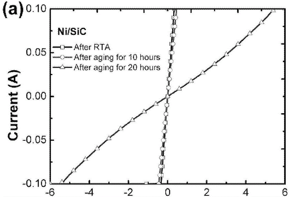
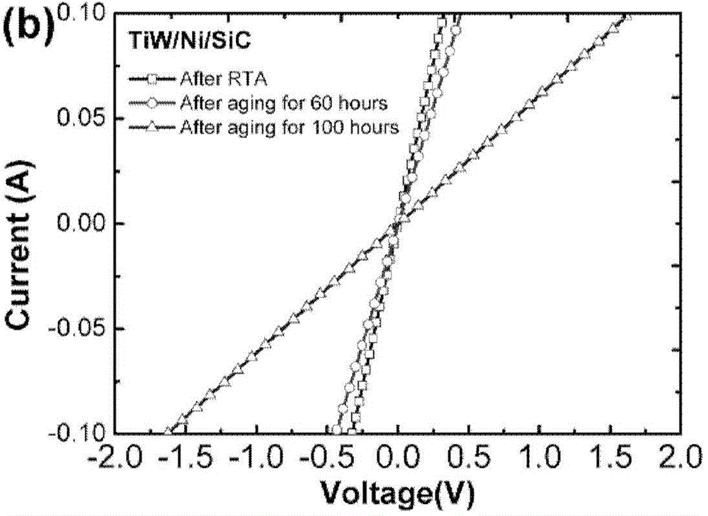
[0027] The invention provides a method for making a SiC ohmic contact by using a TiW / Ni / SiC structure, which is used to improve device reliability. The method is mainly to first deposit ohmic contact metal Ni on the clean SiC surface, then deposit TiW alloy on the deposited ohmic contact layer, and finally perform high-temperature annealing on the semiconductor.

[0028] In order to further illustrate the features and technical solutions of the present invention, the structure, advantages and performance of the present invention will be further described in detail below through the description of specific embodiments in conjunction with the accompanying drawings.

[0029] A kind of method that utilizes TiW / Ni / SiC structur...


PUM


Abstract

The invention discloses a silicon carbide ohmic contact electrode and a manufacturing method of the silicon carbide ohmic contact electrode. The manufacturing method includes the steps of providing a SiC wafer material, and cleaning the surface of a SiC wafer; depositing ohmic contact metal Ni on the surface of the SiC wafer; depositing TiW alloy on the ohmic contact metal Ni; conducting high-temperature annealing on ohmic contacts, and completing manufacturing of SiCohmic contact structures. According to the silicon carbide ohmic contact electrode and the manufacturing method, as the TiW alloy has certain oxidation resistance, ohmic contact partial oxidation efficacy losing in the ohmic contact annealing and follow-up technological process can be prevented; the ohmic contacts of TiW/Ni/SiC structures have the better reliability compared with ohmic contacts of Ni/SiC structures.

Description

technical field [0001] The invention is applicable to the field of manufacturing silicon carbide devices, in particular to a silicon carbide ohmic contact electrode and a manufacturing method thereof. Background technique [0002] Silicon carbide (SiC), as a third-generation semiconductor material, has a high band gap (2.4-3.3eV), high thermal conductivity (5-7W·cm -1 K -1 ), high critical breakdown electric field (>2×10 5 V·cm -1 ), electron mobility equivalent to silicon (Si), stable chemical properties, high hardness, friction resistance, and radiation resistance, etc., have a wide range of applications in high temperature, high frequency, high power, etc. [0003] Ohmic contact is a key process technology in semiconductor manufacturing. Its purpose is to make the voltage drop at the contact of the semiconductor material small enough to not affect the performance of the device when a voltage is applied. If the reliability of the ohmic contact resistance is poor, th...

Claims


Application Information

Patent Timeline
IPC IPC(8): H01L21/28H01L29/45
CPCH01L29/401H01L29/45
Inventor 刘胜北何志刘斌杨香刘兴昉张峰王雷田丽欣刘敏申占伟赵万顺樊中朝王晓峰王晓东赵永梅杨富华孙国胜曾一平
Owner INST OF SEMICONDUCTORS - CHINESE ACAD OF SCI
Why Eureka
Try Eureka