
Three-dimensional integrated sensor chip packaging structure and packaging method

A sensor chip and packaging structure technology, applied in the direction of instruments, electrical digital data processing, electrical components, etc., can solve the problems of wire breakage of the sensor chip and the substrate, reduce product reliability, and can no longer be placed, and achieve enhanced The effect of using function and reliability, reducing package size, reducing overall cost

Active Publication Date: 2017-05-03
HUATIAN TECH KUNSHAN ELECTRONICS
View PDF5 Cites 0 Cited by
  • Summary
  • Abstract
  • Description
  • Claims
  • Application Information

AI Technical Summary

Problems solved by technology

In this form of sensor chip packaging structure, the wire bonding between the sensor chip and the substrate is easily crushed and broken, and no other dielectric layer can be placed above the wire bonding, which affects the packaging yield of the product and reduces the product quality. reliability
Due to the limitation of the wire bonding process, the thickness of the sensor chip package completed by this process is relatively large, which cannot meet the requirement of minimizing the package volume.
In addition, this packaging structure is not conducive to combining with other functional chips, and the sensor chip has a single function

Method used


Image

  • Three-dimensional integrated sensor chip packaging structure and packaging method
  • Three-dimensional integrated sensor chip packaging structure and packaging method
  • Three-dimensional integrated sensor chip packaging structure and packaging method

Examples


Embodiment 1

[0053] Such as Figure 13 As shown, a three-dimensional integrated sensor chip packaging structure includes a sensor chip 1 having opposite first surfaces 101 and second surfaces 102, the first surface 101 has a sensing area 103 and is located around the sensing area 103 Several first welding pads 104, several first welding pads 104 are electrically connected to the sensing area 103, the sensing area is used to receive user fingerprint information, and the first welding pad is used to derive the circuit of the sensing area; A first plastic seal layer 2 exposing the sensing area is formed on the first surface; a first groove 3 is formed on the second surface opposite to each of the first pads, and the second surface is in contact with the first pads. A second groove 4 is formed at the opposite position of the sensing area, a third groove 5 is formed at the bottom of the second groove, and the opening of the third groove is smaller than the bottom area of ​​the second groove, A...

Embodiment 2

[0077] This embodiment 2 includes all the technical features in the embodiment, such as Figure 14 As shown, the difference is that the protective layer in the packaging structure is an insulating protective layer, and optionally, the material of the insulating protective layer is photoresist, which can prevent the metal wiring layer from being oxidized. That is, in Embodiment 1, the second plastic sealing layer is replaced by an insulating protective layer. Preferably, a layer of underfill glue 14 is filled between the sensor chip and the substrate, and the function of the underfill glue is to increase the bonding force between the two.

[0078] The packaging method of the packaging structure of the three-dimensional integrated sensor chip in this embodiment 2 includes the following steps:

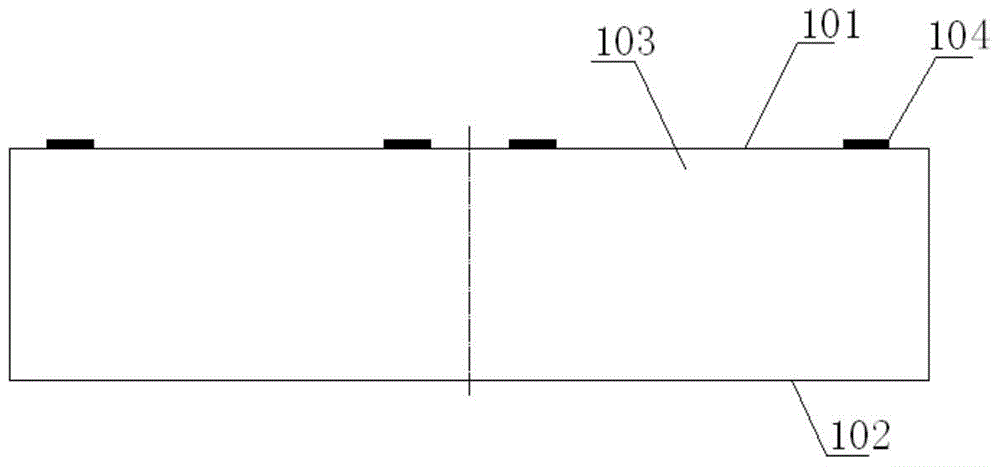
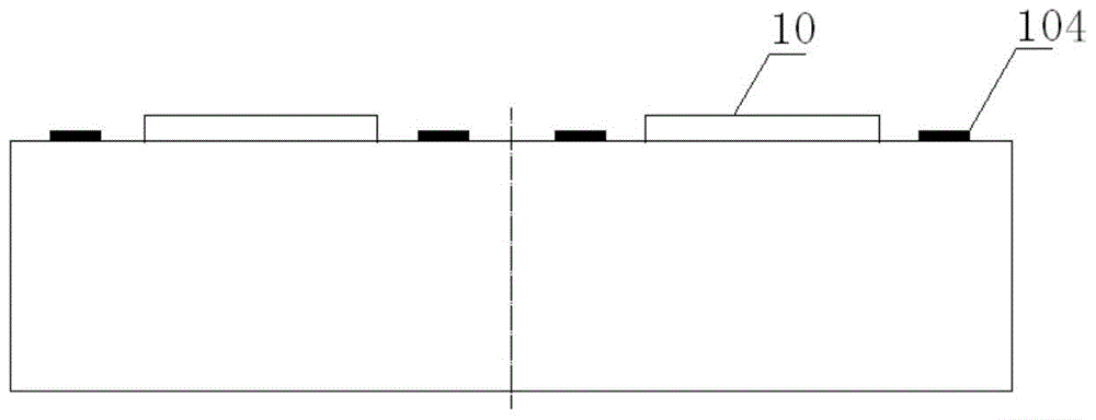
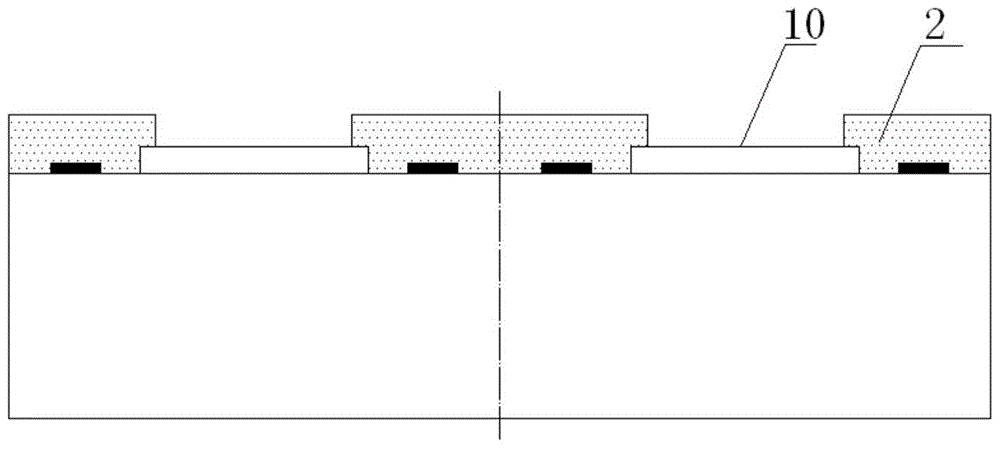
[0079] a. see figure 1 , prepare a wafer with several sensing chip units, each of which has a first surface 101 and a second surface 102 opposite to the first surface; on the first surf...


PUM


Abstract

The invention discloses a three-dimensional integrated sensor chip packaging structure and packaging method. The packaging structure comprises a sensor chip and a substrate. The first surface of the sensor chip is provided with multiple first welding pads and an induction area, a first groove, a second groove and a third groove are carved in the second surface of the sensor chip, insulating layers and metal wiring layers are laid in the first groove, the second groove and the third groove, the sensor chip and a second welding pad on the substrate are connected together through a solder ball in a flip chip mode, and a plastic package layer is arranged on the outer side of the sensor chip. The packaging structure can reduce packaging thickness and meet the requirement for miniaturization development of the sensor chip. The special groove structures in the packaging structure and overall plastic package can be well combined with other functional chips, and use performance and reliability of the chips are enhanced. According to the packaging method, a wafer level chip size packaging technology is used, overall packaging is carried out firstly, then a wafer is cut into single chips, and accordingly production cost is lowered.

Description

technical field [0001] The invention relates to a wafer-level chip size packaging structure and technology, in particular to a three-dimensional integrated sensor chip packaging structure and packaging method. Background technique [0002] Sensor chips or sensor chips, such as fingerprint recognition sensor chips, touch sensor chips, etc., have been continuously expanded due to their simplicity and practicability. Smart terminal devices with increasingly powerful functions are also beginning to carry more and more sensor chips. However, current devices have higher requirements for short, light and thin packaging devices, and the packaging volume of such sensor chips equipped with them will also be pursued. minimize. [0003] However, conventional wafer-level sensor chip size packaging usually uses a wire bonding process to connect the sensor chip to the substrate. The specific structure is: the sensor chip has a first surface and a second surface opposite to the first surfa...

Claims


Application Information

Patent Timeline
Patent Type & Authority Patents(China)
IPC IPC(8): H01L23/485H01L21/60G06K9/00G06F3/041
CPCH01L24/97H01L2224/48091
Inventor 万里兮黄小花沈建树王晔晔钱静娴翟玲玲
Owner HUATIAN TECH KUNSHAN ELECTRONICS
Learn More