PMOS structure with SiGe source and drain area and manufacturing method thereof

A manufacturing method and technology for source and drain regions, which are applied in semiconductor/solid-state device manufacturing, electrical components, circuits, etc., can solve the problems of NiSi growth difficulties, stress relaxation, and device performance deterioration, and achieve enhanced device yield and improved device performance. stress, the effect of improving device performance

Inactive Publication Date: 2015-04-22
SHANGHAI INTEGRATED CIRCUIT RES & DEV CENT
View PDF4 Cites 1 Cited by
  • Summary
  • Abstract
  • Description
  • Claims
  • Application Information

AI Technical Summary

Problems solved by technology

[0006] However, in the epitaxial process of SiGe with high Ge concentration, due to the sudden change of Ge concentration at the interface between the SiGe buffer layer and the SiGe main layer, and between the SiGe main layer and the Si cap layer, defects such as dislocations will be generated at the interface. like Figure 4 shown
Dislocations will cause stress relaxation, resulting i

Method used


Image

  • PMOS structure with SiGe source and drain area and manufacturing method thereof
  • PMOS structure with SiGe source and drain area and manufacturing method thereof
  • PMOS structure with SiGe source and drain area and manufacturing method thereof

Examples


Example Embodiment

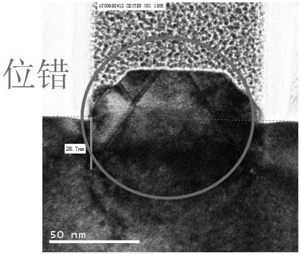
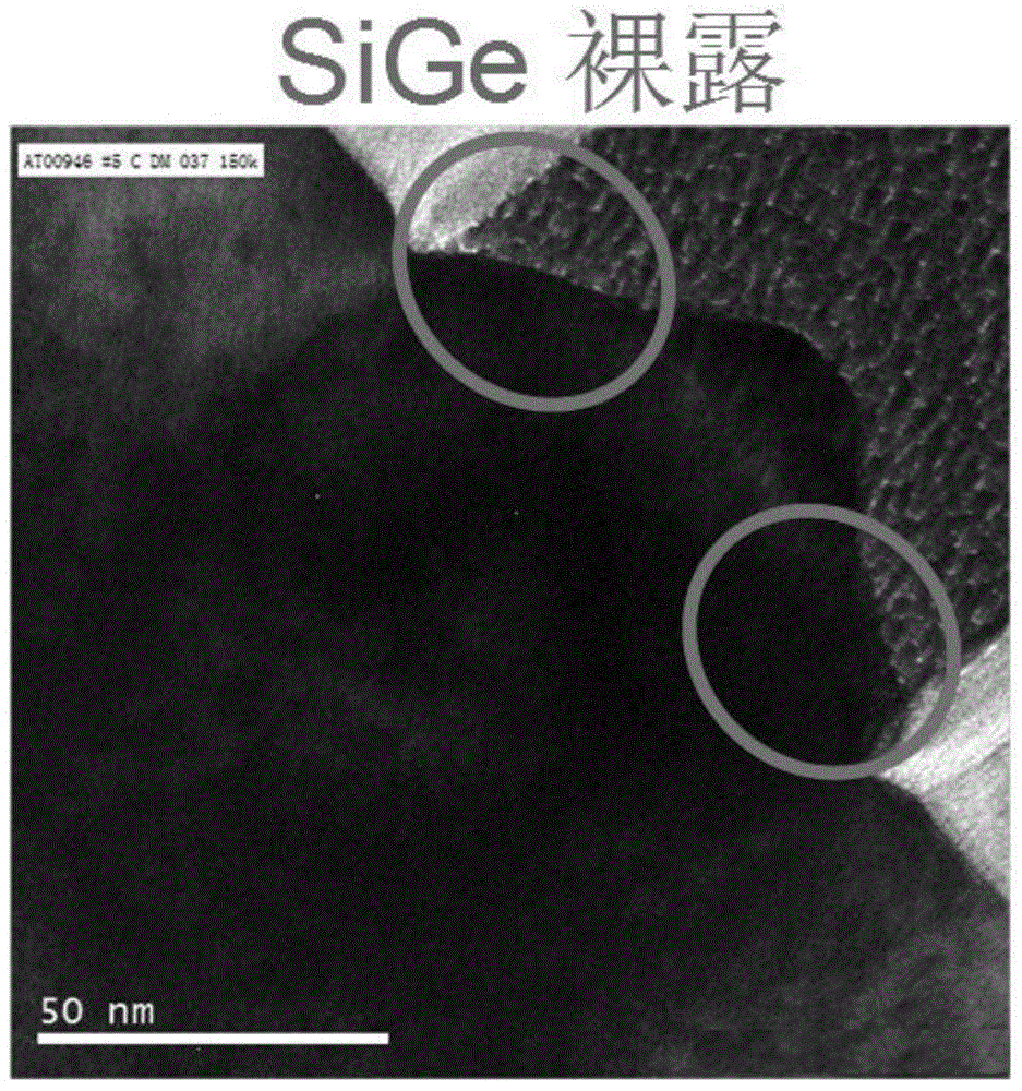
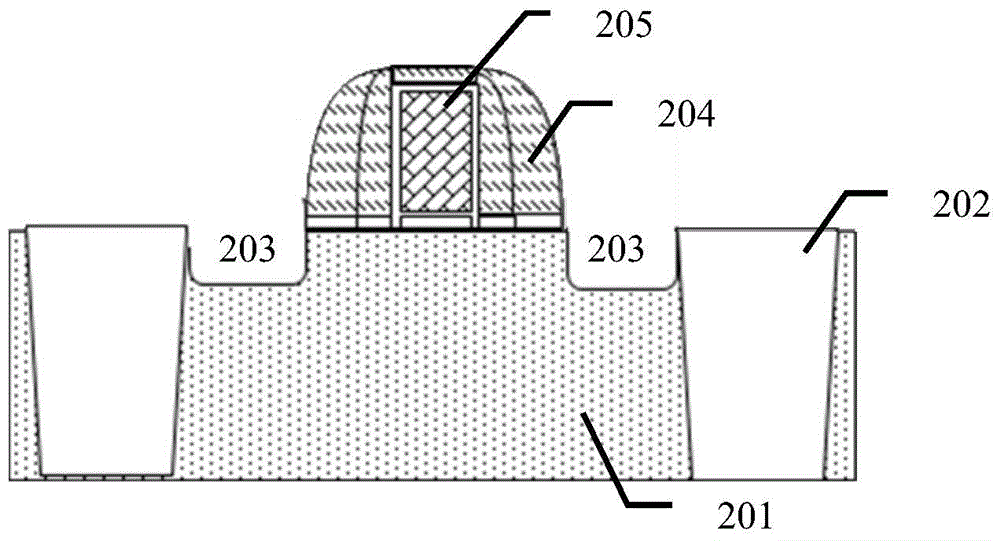
[0036] see Image 6 , the PMOS structure with SiGe source and drain regions in this embodiment includes a substrate 101, a gate 104 on the substrate 101, and source and drain regions on both sides of the gate 104 and between the shallow trench isolation 102, the source and drain regions Manufactured in the etched groove 103, the source and drain regions sequentially include a SiGe buffer layer 105, a SiGe body layer 106, and a Si cap layer 107 from bottom to top, wherein the SiGe body layer includes a first body layer from bottom to top and the second body layer, the Ge concentration of the first body layer increases from bottom to top, and the Ge concentration of the second body layer decreases from bottom to top, and the highest Ge concentration of the two is the same.

[0037] In this embodiment, through the above-mentioned settings, the first main body layer with increasing Ge concentration and the second main body layer with decreasing Ge concentration are arranged in the...


PUM


Abstract

The invention discloses a PMOS structure with a SiGe source and drain area. A first main layer with the Ge concentration gradually increased and a second main layer with the Ge concentration gradually reduced are arranged in a SiGe main layer, the change of gradient of the Ge concentration is formed so that dislocation and stress release caused by the sudden change of the Ge concentration at the interface position of the main layer and a buffering layer can be avoided, the low Ge concentration is restored at the interface position of the main layer and a cap layer and serves as the growth end concentration, and therefore it is ensured that the cap layer well wraps the main layer. The highest position of Ge concentration is the interface layer of the first main layer and the second main layer or the middle layer position in the middle and used for improving the stress of a channel, and therefore the yield of devices is increased, and the performance of the devices is improved.

Description

technical field [0001] The invention relates to the technical field of semiconductor integrated circuit manufacturing technology, in particular to a PMOS structure with SiGe source and drain regions and a manufacturing method thereof. Background technique [0002] With the development of semiconductor integrated circuits, the size reduction of MOSFET (Metal Oxide Semiconductor Field Effect Transistor) has continuously improved the speed, performance, density and functional unit cost of integrated circuits. After entering the 90nm technology era, with the substantial reduction in the size of integrated circuit devices, the junction depth of the source / drain (elevated source / drain) is getting shallower and shallower, and it is necessary to use selective epitaxy technology (selective epi SiGe, abbreviated as SEG) to increase Thick source / drain, where the Si capping layer can protect SiGe, and serve as a sacrificial layer for subsequent silicide reactions, thereby reducing serie...

Claims


Application Information

Patent Timeline
IPC IPC(8): H01L29/78H01L29/08H01L21/336
CPCH01L29/78H01L29/06H01L29/66477
Inventor 钟旻
Owner SHANGHAI INTEGRATED CIRCUIT RES & DEV CENT
Why Eureka
Try Eureka