Chemical nickel-palladium alloy plating process for circuit boards

A technology of electroless nickel plating and nickel palladium alloy, applied in liquid chemical plating, metal material coating process, coating and other directions, can solve problems such as complex process, and achieve the effect of reducing manufacturing cost, high hardness and ensuring performance.

Active Publication Date: 2015-04-29
广东致卓环保科技有限公司
View PDF3 Cites 13 Cited by
  • Summary
  • Abstract
  • Description
  • Claims
  • Application Information

AI Technical Summary

Problems solved by technology

The first four surface treatments all have certain defects. In recent years, the popular chemical nickel-palladium-gold process has been widely used because the coating has good wear resistance and corrosion resistance and can be welded. However, the expensive precious metal Au is used, and the process slightly complicated

Method used


Image

  • Chemical nickel-palladium alloy plating process for circuit boards
  • Chemical nickel-palladium alloy plating process for circuit boards
  • Chemical nickel-palladium alloy plating process for circuit boards

Examples


Embodiment 1

[0037] Present embodiment is to be base material with copper sheet, test according to described steps; Wherein, the composition of the nickel-palladium alloy plating solution that step 7 adopts comprises:

[0038]

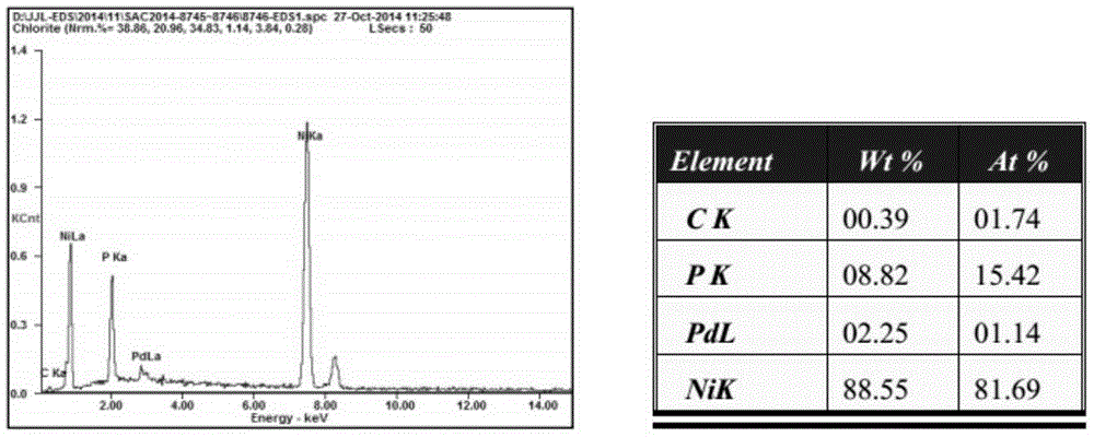
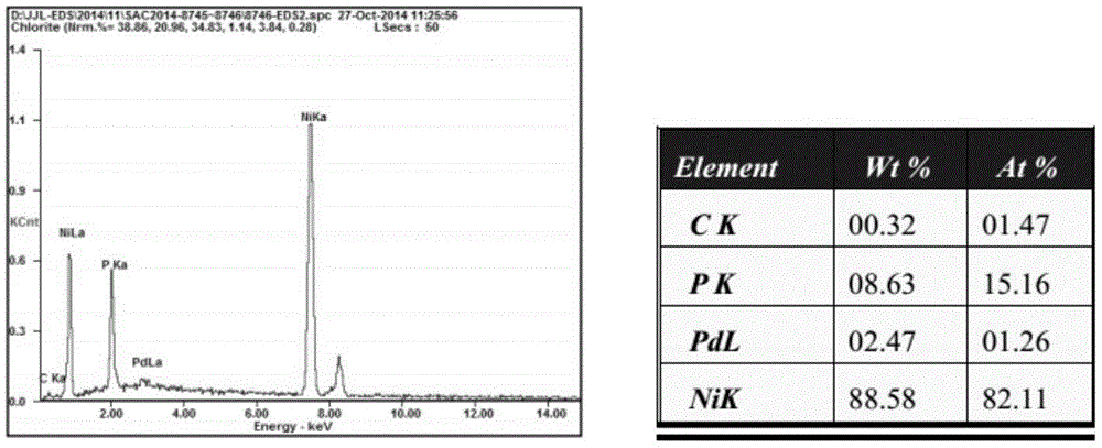
[0039] The SEM test was carried out on the sample, and the microscopic appearance of the obtained coating was as follows: figure 1 , EDS test obtained coatings and scanning patterns such as figure 2 and image 3 .

Embodiment 3

[0041] Present embodiment is to be base material with copper sheet, test according to above-mentioned steps; Wherein, the composition of the nickel-palladium alloy plating solution that step 7 adopts comprises:

[0042]

[0043]

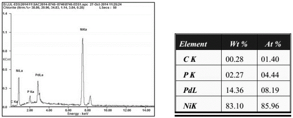
[0044] The SEM test was carried out on the sample, and the microscopic appearance of the obtained coating was as follows: Figure 4 , EDS test obtained coatings and scanning patterns such as Figure 5 and Image 6 .


PUM


Abstract

The invention discloses a chemical nickel-palladium alloy plating process for circuit boards. The chemical nickel-palladium alloy plating process is characterized by comprising the following steps: (1) degreasing: placing a circuit board in an acidic degreasing agent to remove greasy dirt and fingerprints on the surface of the circuit board; (2) microetching: placing the degreased circuit board in microetching liquid to slightly etch the copper surface; (3) activation: placing the micro-etched circuit board in a palladium activating liquid to be activated, so that a layer of activated palladium is deposited on the surface of the circuit board; (4) chemical nickel plating: placing the activated circuit board in nickel plating liquid so as to deposit a layer of nickel on the copper surface; (5) microetching: placing the circuit board plated with nickel in acid liquid so as to slightly etch the nickel surface; (6) activation: placing the micro-etched circuit board in the palladium activating liquid to be activated, so that a layer of activated palladium is deposited on the surface of the circuit board; (7) chemical nickel-palladium plating: placing the activated circuit board in nickel-palladium alloy plating liquid to be plated, and depositing a nickel-palladium alloy plated layer on the nickel surface; (8) washing and drying the circuit board: washing the board surface to remove medicine liquids in former preparation processes, and drying. Through the adoption of the chemical nickel-palladium alloy plating process disclosed by the invention, the production cost can be reduced effectively, and the application of the surface treatment process of circuit boards is facilitated.

Description

technical field [0001] The invention relates to a circuit board surface treatment process, which is an electroless nickel-palladium alloy plating process for the circuit board. Background technique [0002] At present, the surface treatments suitable for circuit boards mainly include: 1. Organic solder protectant; 2. Displacement silver plating; 3. Displacement tin plating; 4. Chemical nickel / displacement gold plating; Pd / Au) process. The first four surface treatments all have certain defects. In recent years, the popular chemical nickel-palladium-gold process has been widely used because the coating has good wear resistance and corrosion resistance and can be welded. However, the expensive precious metal Au is used, and the process Slightly complicated. Therefore, it is necessary to provide an alternative process for the gold layer on the surface of the circuit board. Contents of the invention [0003] The purpose of the present invention is to provide a kind of electr...

Claims


Application Information

Patent Timeline
Patent Type & Authority Applications(China)
IPC IPC(8): C23C18/18C23C18/36C23C18/50
CPCC23C18/1655C23C18/18C23C18/36C23C18/50
Inventor 谢金平赖福东范小玲陈世荣徐振宇曹权根
Owner 广东致卓环保科技有限公司
Why Eureka
Try Eureka