

Transistor small signal equivalent circuit model
An equivalent circuit model, small-signal technology, applied in electrical digital data processing, special data processing applications, instruments, etc., can solve the problem that high-order parasitic effects are not considered, and the small-signal equivalent circuit model of transistors cannot accurately characterize parasitic effects and other problems to achieve the effect of high-precision performance
- Summary
- Abstract
- Description
- Claims
- Application Information
AI Technical Summary
Problems solved by technology
Method used
Image

Examples
Embodiment 1
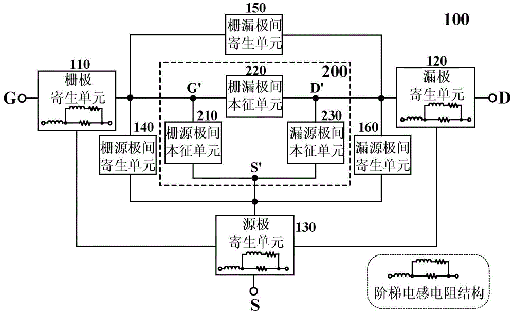
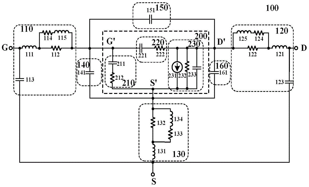
[0033] Embodiment 1: as figure 1 As shown, the small-signal equivalent circuit model of a field effect transistor includes a parasitic part 100 (outside the dotted line) and an intrinsic part 200 (inside the dotted line). The intrinsic part includes the gate-source intrinsic unit 210 located between the gate internal node G` and the source internal node S`, and the gate-drain cell 210 located between the gate internal node G` and the drain internal node D` The intrinsic cell 220 is located at the drain-source intrinsic cell 230 between the inner source node S′ and the inner drain node D′.
[0034] The source external node S is connected outside the source internal node S′, the drain external node D is connected outside the drain internal node D′, and the gate external node G is connected outside the gate internal node G′.
[0035] The parasitic part includes a source parasitic unit 130 located between the source inner node S′ and the source outer node S, a source parasitic un...
Embodiment 2
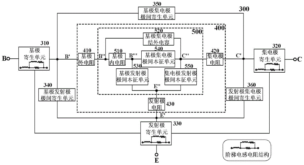
[0057] Embodiment 2: as figure 2 As shown, the small-signal equivalent circuit model of a bipolar transistor includes a parasitic part 300 , an external resistance part 400 and an intrinsic part 500 . The equivalent circuit model has base parasitic node B, base external resistance node B`, base junction outer node B`` and base junction inner node B``` in series; emitter parasitic node in series E. Emitter external resistor node E`, emitter node E``; collector parasitic node C, collector external resistor node C`, collector node C`` connected in series.
[0058] Wherein the intrinsic part 500 includes the base internal resistance 510 connected between the base junction inner node B``` and the base junction outer node B``; the base junction inner node B``` is connected to the collector junction Base-collector inter-electrode intrinsic unit 540 between nodes C``; base-collector extra-junction capacitance 520 connected between base-external node B`` and collector node C``; The ...
PUM
 Abstract
Description
Claims
Application Information