Tunnel-type hardening furnace for semiconductor device

A hardening furnace and semiconductor technology, applied in the fields of semiconductor devices, semiconductor/solid-state device manufacturing, electrical components, etc., can solve the problems of inconsistent product quality, low efficiency, uneven heating temperature and time control, and save labor and temperature. effective effect

Active Publication Date: 2015-04-29
广东歌得智能装备有限公司
View PDF7 Cites 7 Cited by
  • Summary
  • Abstract
  • Description
  • Claims
  • Application Information

AI Technical Summary

Problems solved by technology

[0004] The purpose of the present invention is to provide a rapid heating and hardening equipment for semiconductor components, which aims to solve the problem that the existing rapid heating and hardening process requires manual processing, which cannot ensure consistency and low efficiency. In addition, uneven heating temperature and time control lead to inconsistent product quality technical issues

Method used


Image

  • Tunnel-type hardening furnace for semiconductor device
  • Tunnel-type hardening furnace for semiconductor device
  • Tunnel-type hardening furnace for semiconductor device

Examples


Embodiment Construction

[0030] In order to make the object, technical solution and advantages of the present invention more clear and definite, the present invention will be further described below with reference to the accompanying drawings and examples.

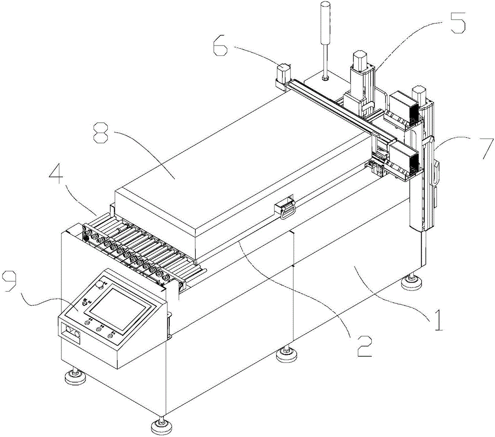
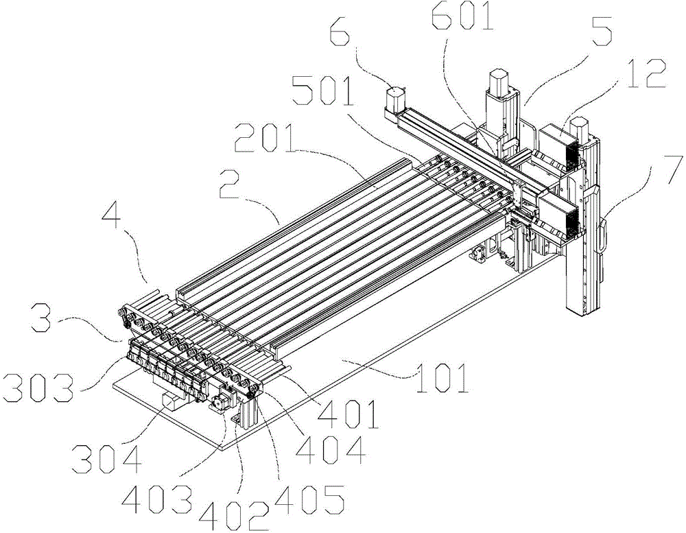
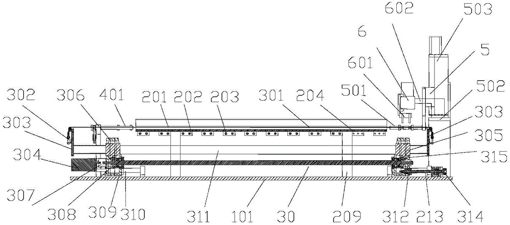
[0031] see figure 1 and figure 2 , the equipment provided by the present invention mainly includes: a hardening furnace base 1, a heating platform 2, a conveying mechanism 3, a furnace cover 8 and an electric control platform 9, the heating platform 2 is arranged on the hardening furnace base 1, and is used for semiconductor Device heating; the conveying mechanism 3 is set across the two ends of the heating platform 2, and the semiconductor device is transported to the heating platform 2 through a steel wire as a conveying tool; the furnace cover 8 is arranged on the heating platform 2 for use in the hardening furnace A tunnel-type heating chamber is formed on the base 1; the electric control platform 9 is electrically connected with the heating...


PUM


Abstract

The invention discloses a tunnel-type hardening furnace for a semiconductor device. The tunnel-type hardening furnace for the semiconductor device is characterized by comprising a hardening surface base platform, a heating platform, a conveying mechanism, a furnace cover and an electric control platform, wherein the heating platform is arranged on the hardening surface base platform and is used for heating the semiconductor device; the conveying mechanism spans over two ends of the heating platform and conveys the semiconductor device to the heating platform by using a steel wire as a conveying tool; the furnace cover is arranged on the heating platform and is used for forming a tunnel-type heating chamber in the hardening surface base platform; the electric control platform is electrically connected with the heating platform and the conveying mechanism and is used for controlling heating and automatic conveying of the hardening furnace. According to the tunnel-type hardening furnace for the semiconductor device, manpower can be saved, the production efficiency can be improved, and meanwhile, the consistency of product quality is controlled.

Description

technical field [0001] The invention relates to the field of heating and hardening technology of electronic components, in particular to a tunnel type hardening furnace for semiconductor devices, especially for the rapid shaping process of LED packaging. Background technique [0002] At present, many electronic components need to undergo heating and hardening process during production and processing. Taking LED as an example, the common white LED uses the light generated by the blue chip to excite the phosphor to emit yellow-green light, which is matched with the blue light of the LED chip to produce white light. Phosphor powder is generally coated on the blue LED chip by dispensing process, and then hardened and formed. During the hardening process, due to the large specific gravity of the phosphor powder, sedimentation will occur in the liquid encapsulant, and the absorption and scattering characteristics of the phosphor layer for blue light will change greatly, resulting...

Claims


Application Information

Patent Timeline
Patent Type & Authority Applications(China)
IPC IPC(8): H01L21/67H01L33/00
CPCH01L21/67098H01L21/67121H01L33/00
Inventor 单忠频康茂陈树钊陈伟明陈志敏
Owner 广东歌得智能装备有限公司
Why Eureka
Try Eureka