Self-Aligned Contact Hole Etching Method

A self-aligned contact hole and gate contact technology, which is applied in electrical components, semiconductor/solid-state device manufacturing, circuits, etc., can solve the problems that the contact hole is not easy to be fully opened, the process difficulty is increased, and the trench structure is not easily filled. Achieve the effect of reducing the difficulty of PSG filling, enhancing the etching ability and improving the etching quality

Active Publication Date: 2017-08-08
SHANGHAI HUAHONG GRACE SEMICON MFG CORP
View PDF5 Cites 0 Cited by
  • Summary
  • Abstract
  • Description
  • Claims
  • Application Information

AI Technical Summary

Problems solved by technology

[0009] In the existing method, when the self-aligned contact hole 109 on the source-drain region 105 is formed by etching, the self-aligned contact hole 109 will bridge a certain distance d on the silicon nitride sidewall 107, so that the self-aligned contact hole 109 will be formed during etching. The contact hole 109 will cause some damage to the silicon nitride sidewall 107
In addition, when the gate sidewall is formed by the existing method, the thickness of the silicon nitride sidewall 107 on the sidewall of the gate structure will also have a certain loss, and the thickness a of the bottom of the silicon nitride sidewall 107 will always be greater than that of the top. Thickness b
In order to maintain the top thickness b of the silicon nitride spacer 107, the existing method is to increase the thickness of the hard mask layer 106. The increase in the thickness of the hard mask layer 106 will increase the thickness of the entire gate structure. When the gate When the pole spacing c is small, the trench structure between the gate structures will have a larger aspect ratio, which will make it difficult to fill the trench structure between the gate structures during PSG deposition in the subsequent step 4, increasing the Process difficulty; in addition, when the gate spacing c is small, the subsequent self-aligned contact hole etching window will be too small, and the contact hole is not easy to be completely opened to form defects

Method used


Image

  • Self-Aligned Contact Hole Etching Method
  • Self-Aligned Contact Hole Etching Method
  • Self-Aligned Contact Hole Etching Method

Examples


Embodiment Construction

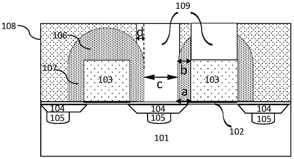
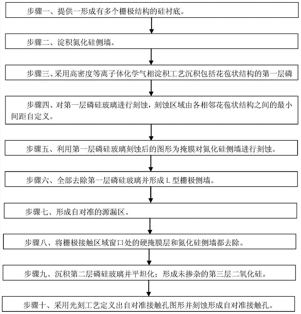
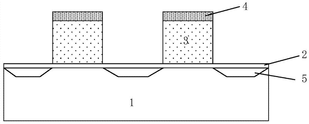
[0030] Such as figure 2 Shown is the flow chart of the method of the embodiment of the present invention; Figure 3A to Figure 3G Shown is a cross-sectional view of the self-aligned contact hole structure in each step of the method of the embodiment of the present invention. The method for etching a self-aligned contact hole in the embodiment of the present invention includes the following steps:

[0031] Step 1, such as Figure 3AAs shown, a silicon substrate 1 formed with a plurality of gate structures is provided, and the gate structure includes a gate dielectric layer 2, a gate polysilicon 3 and a hard mask layer 4 sequentially formed on the surface of the silicon substrate 1 , the pattern of the gate structure is defined by the hard mask layer 4, that is, the pattern of the gate structure is defined by the hard mask layer 4 and all operations are performed under the protection of the hard mask layer 4 etching of the gate polysilicon 3; self-aligned lightly doped drain...


PUM


Abstract

The invention discloses a method for etching a self-aligned contact hole, which comprises the steps of: providing a silicon substrate formed with a plurality of gate structures; depositing silicon nitride side walls; A layer of phosphosilicate glass; the first layer of phosphosilicate glass is etched, and the etched area is defined by the minimum distance between adjacent flower-shaped structures; the etched pattern of the first layer of phosphosilicate glass is used as a mask pair The silicon nitride sidewall is etched; the first layer of phosphosilicate glass is completely removed and the L-shaped gate sidewall is formed; the self-aligned source and drain regions are formed; the hard mask layer and nitride at the window of the gate contact area All silicon sidewalls are removed; a second layer of phosphosilicate glass is deposited and planarized; an undoped third layer of silicon dioxide is formed; a photolithographic process is used to define a self-aligned contact hole pattern and etched to form a self-aligned contact hole. The invention can reduce the height of the gate structure, increase the distance between the gates, reduce the difficulty of PSG filling between the gate structures, enhance the etching ability of the self-aligned contact hole, and improve the etching quality of the self-aligned contact hole.

Description

technical field [0001] The invention relates to a semiconductor integrated circuit manufacturing process method, in particular to a self-aligned contact hole etching method. Background technique [0002] Such as figure 1 Shown is a cross-sectional view of a self-aligned contact hole structure formed by an existing self-aligned contact hole etching method; the existing self-aligned contact hole etching method includes the following process steps: [0003] Step 1: Provide a silicon substrate 101 formed with a plurality of gate structures, the gate structure includes a gate dielectric layer 102, a gate polysilicon 103 and a hard mask layer 106 sequentially formed on the surface of the silicon substrate 101 The pattern of the gate structure is defined by the hard mask layer 106; self-aligned lightly doped drain regions 104 are formed in the silicon substrate 101 on both sides of each gate structure. The gate dielectric layer 102 can be a gate oxide layer, and the gate polysili...

Claims


Application Information

Patent Timeline
Patent Type & Authority Patents(China)
IPC IPC(8): H01L21/768H01L21/311
Inventor 郭振强陈瑜罗啸马斌陈华伦
Owner SHANGHAI HUAHONG GRACE SEMICON MFG CORP
Why Eureka
Try Eureka