Thin-film transistor structure

A thin-film transistor and film-forming technology, which is applied in the field of thin-film transistor structure, can solve the problems of increased leakage current of thin-film transistors and affect the gray scale of the display screen, etc., and achieve the effect of reducing contact barrier, reducing leakage current, and good ohmic contact

Inactive Publication Date: 2015-04-29
TRULY HUIZHOU SMART DISPLAY
View PDF5 Cites 15 Cited by
  • Summary
  • Abstract
  • Description
  • Claims
  • Application Information

AI Technical Summary

Problems solved by technology

However, in the subsequent high-temperature process, highly doped phosphorus will diffuse into the semiconductor layer, which will increase the leakage current of the thin film transistor, thereby affecting the gray scale of the display screen.

Method used


Image

  • Thin-film transistor structure
  • Thin-film transistor structure
  • Thin-film transistor structure

Examples


no. 1 example

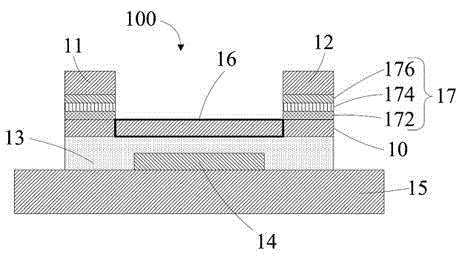
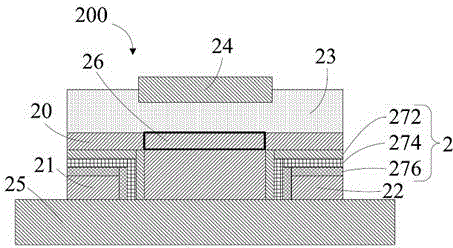
[0048] Compared with the first embodiment, the difference in this embodiment is only that: the semiconductor layer 20 is disposed on the surface of the insulating substrate 25, the source electrode 21 and the drain electrode 22 are disposed on the surface of the semiconductor layer 20 at intervals, The insulating layer 23 is disposed on the surface of the semiconductor layer 20 . The gate 24 is disposed on the surface of the insulating layer 23, and is insulated from the semiconductor layer 20, the source 21 and the drain 22 through the insulating layer 23. A channel 26 is formed in a region of the semiconductor layer 20 between the source 21 and the drain 22 .

[0049] The source 21 and the drain 22 can be arranged at intervals on the lower surface of the semiconductor layer 20, between the insulating substrate 25 and the semiconductor layer 20, at this time, the source 21, the drain 22 and the gate 24 are disposed on different surfaces of the semiconductor layer 20 to form ...


PUM


Abstract

The invention discloses a thin-film transistor structure. The thin-film transistor structure comprises a source, a drain, a semiconductor layer and a grid, wherein the drain and the source are arranged at an interval; the grid is arranged in an insulation manner relative to the semiconductor layer, the source and the drain through an insulation layer; an ohmic contact layer is further arranged between the semiconductor layer and the source and the drain, and the ohmic contact layer further comprises a first phosphorus-doped layer, a second phosphorus-doped layer and a third phosphorus-doped layer which are stacked, wherein the first phosphorus-doped layer is close to the semiconductor layer, the third phosphorus-doped layer is close to the source and the drain, the phosphorus doping concentration of the first phosphorus-doped layer is lower than that of the second phosphorus-doped layer, and the phosphorus doping concentration of the second phosphorus-doped layer is lower than that of the third phosphorus-doped layer. The thin-film transistor structure disclosed by the invention can reduce a contact potential barrier between a semiconductor and a metal to form good ohmic contact between the two and further effectively reduce the drain current of the amorphous silicon thin-film transistor without affecting the on-state current.

Description

technical field [0001] The invention relates to the technical field of semiconductor manufacturing, in particular to a thin film transistor structure. Background technique [0002] Thin Film Transistor (TFT) is a key electronic component in modern microelectronics technology, and has been widely used in flat panel displays and other fields. Amorphous silicon thin film transistor is the core device of thin film transistor liquid crystal display (TFT-LCD) and active matrix organic light emitting diode panel (AMOLED), and its field effect mobility is very critical. [0003] Currently, existing thin film transistors mainly include a gate, an insulating layer, a source and a drain. In order to reduce the contact barrier between the source and drain metal layer and the semiconductor layer a-Si:H (amorphous silicon), a layer of phosphorus-doped n+a-Si (phosphorus) is usually added between the source and drain metal layer and the semiconductor layer. Doped layer) to form a good oh...

Claims


Application Information

Patent Timeline
Patent Type & Authority Applications(China)
IPC IPC(8): H01L29/786H01L29/423
CPCH01L29/78696H01L29/78669
Inventor 胡典禄陈建荣任思雨苏君海黄亚清李建华
Owner TRULY HUIZHOU SMART DISPLAY
Why Eureka
Try Eureka