

Preparation of passivation tunneling layer material and application thereof in solar cell
A technology of solar cells and tunneling layers, which is applied in the manufacture of circuits, electrical components, and final products, and can solve problems affecting the potential of structural batteries
- Summary
- Abstract
- Description
- Claims
- Application Information
AI Technical Summary
Problems solved by technology
Method used
Image

Examples
preparation example Construction
[0073] The preparation method of the carrier passivation tunneling film may include the steps of: using magnetron sputtering (Sputter), plasma enhanced chemical vapor deposition (PECVD), thermal evaporation (Thermal Evaporator), electron beam evaporation (E-beamEvaporator ), low-pressure chemical vapor deposition (LPCVD) or atomic layer deposition (ALD) methods, deposit tantalum pentoxide (Ta 2 o 5 ), thereby forming the carrier passivation tunneling film.
[0074] The preparation method of the carrier passivation tunneling film may include the following steps:
[0075] (a) In the vacuum chamber containing the silicon wafer, the pressure of the vacuum chamber is lower than 10 -2 Torr, pass into the gas containing tantalum (Ta) precursor molecule; Wherein, pass through time is 0.5-5 second; Preferably, be 1 second;
[0076] (b) feed an inert gas; wherein, the feed time is 10-60 seconds; preferably, 20-35 seconds; the flow rate of the inert gas is 50-200 sccm; preferably, 80-...
Embodiment 1
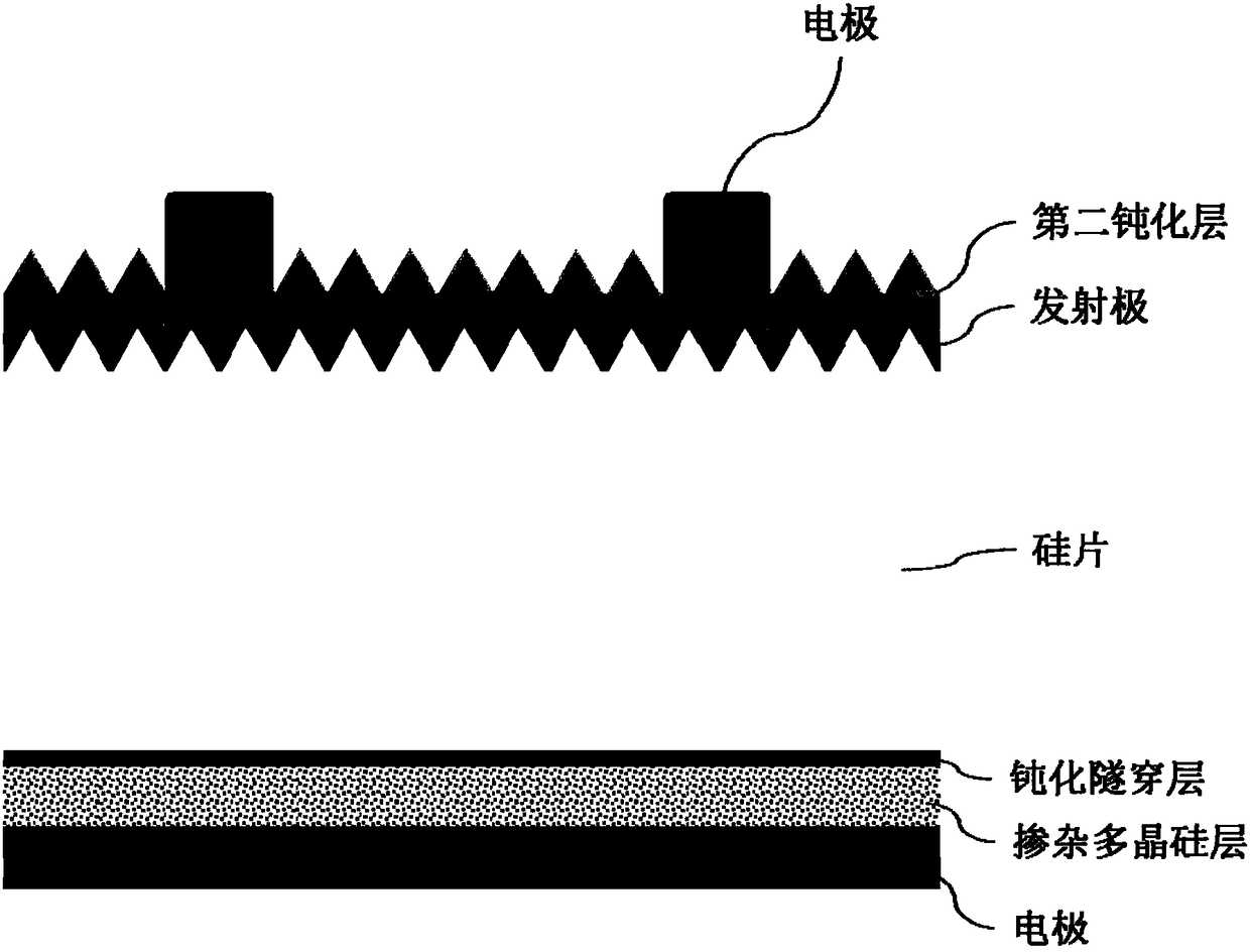
[0122] Step (1): Using a p-type monocrystalline silicon wafer with a resistivity of 2.0 Ω cm as the substrate, deposit Ta on both sides of the silicon wafer by atomic layer deposition (ALD) 2 o 5 film. Specific method: put the silicon wafer cleaned by RCA standard process into the ALD cavity, pump the cavity pressure to 10 -2 Below Torr, while heating the chamber to 200°C. Using tantalum ethoxide and water as precursors, first pass tantalum ethoxide vapor for 1 second, then pass nitrogen gas with a flow rate of 100 sccm for 30 seconds, then pass water vapor for 1 second, and finally pass nitrogen gas with a flow rate of 100 sccm for 30 seconds , which is a cycle. After 60 cycles of treatment, 1.8±0.2nm Ta can be obtained on the surface of the silicon wafer 2 o 5 film.
[0123] Step (2): Using aluminum particles as the evaporation source, in the prepared Ta 2 o 5 An aluminum electrode is vapor-deposited on the surface of the film with a specific mask pattern, and the th...
Embodiment 2
[0130] Step (1): Using a p-type monocrystalline silicon wafer with a resistivity of 2.0 Ω cm as the substrate, deposit Ta on both sides of the silicon wafer by atomic layer deposition (ALD) 2 o 5 film. Concrete method is with embodiment 1 step (1)
[0131] Step (2): Subsequent deposition of Ta on both sides by PECVD method 2 o 5 A boron-doped amorphous silicon film is deposited on both sides of the film sample. The specific method is: deposit Ta on both sides 2 o 5 The sample of the thin film is transferred to the PECVD chamber, and the chamber pressure is pumped to 10 - 5 below Torr while heating the sample to 150°C. Pass into 10sccm high-purity silane (SiH 4 ) and 10 sccm hydrogen diluted diborane (3% B 2 h 6 ), a radio frequency power of 10W, a process pressure of 0.4Torr, and a time of 10min, a boron-doped amorphous silicon film of about 40nm can be obtained on the sample surface.
[0132] Step (3): The above prepared double-sided Ta 2 o 5 The samples of thin...
PUM
| Property | Measurement | Unit |
|---|---|---|
| thickness | aaaaa | aaaaa |
| electrical resistivity | aaaaa | aaaaa |
| thickness | aaaaa | aaaaa |
Abstract
Description
Claims
Application Information