Ohm contact production method of semi-insulation SiC semiconductor device
A technology of ohmic contact and manufacturing method, which is applied in the field of microelectronics, can solve the problem of low specific contact resistance of semi-insulating SiC, achieve good matching, facilitate manufacturing, and reduce the effect of contact barrier
- Summary
- Abstract
- Description
- Claims
- Application Information
AI Technical Summary
Problems solved by technology
Method used
Image

Examples
Embodiment 1
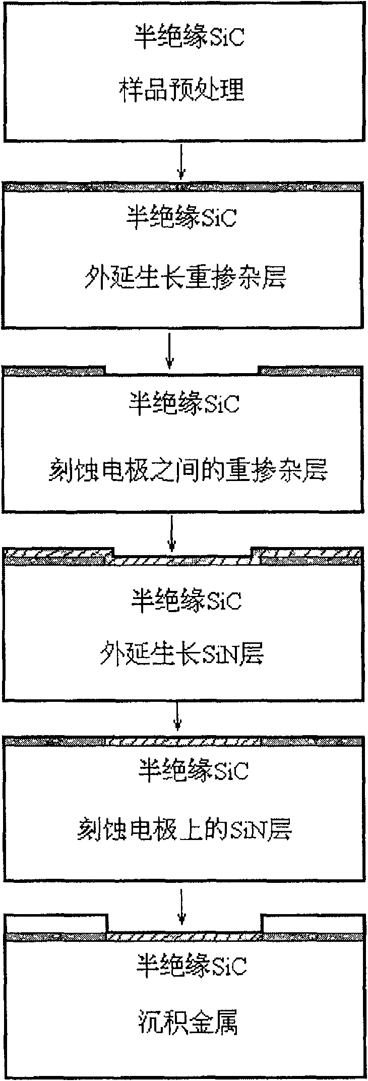
[0027] Embodiment 1, taking a semi-insulating 4H-SiC photoconductive switch as an example, describes in detail the specific process of making an ohmic contact of a semi-insulating 4H-SiC semiconductor device according to the present invention.
[0028] refer to figure 1 , the present invention makes the ohmic contact process on the semi-insulating 4H-SiC photoconductive switch as follows:
[0029] In step 1, pretreatment is performed on the semi-insulating 4H-SiC material used.
[0030] First, passivate the surface of the semi-insulating 4H-SiC substrate with molten KOH. The etching temperature and etching time are 210°C and 15s, respectively; then, the passivated wafer is sequentially treated with acetone, methanol, and deionized water. Clean the sample, and finally, use the RCA standard cleaning process to remove the oxide layer on the surface of the substrate.
[0031] Step 2, epitaxially growing a heavily doped layer.
[0032] The heavily doped GaN heavily doped layer i...
Embodiment 2
[0060] In Embodiment 2, a semi-insulating 3C-SiC photoconductive switch is taken as an example.
[0061] The steps of using the heavily doped layer to make its ohmic contact are the same as the scheme 1 of Example 1, the only difference is that in step 2, a p-type GaN heavily doped layer is used for the deep main compensation type semi-insulating 4H-SiC, and the doping dose is 2.875×10 19 , the optimal doping thickness is 71.88nm; for deep donor compensated semi-insulating SiC, an n-type GaN heavily doped layer is used, and the doping dose is 2.73×10 19 , the optimum thickness of doping is 71.88nm.
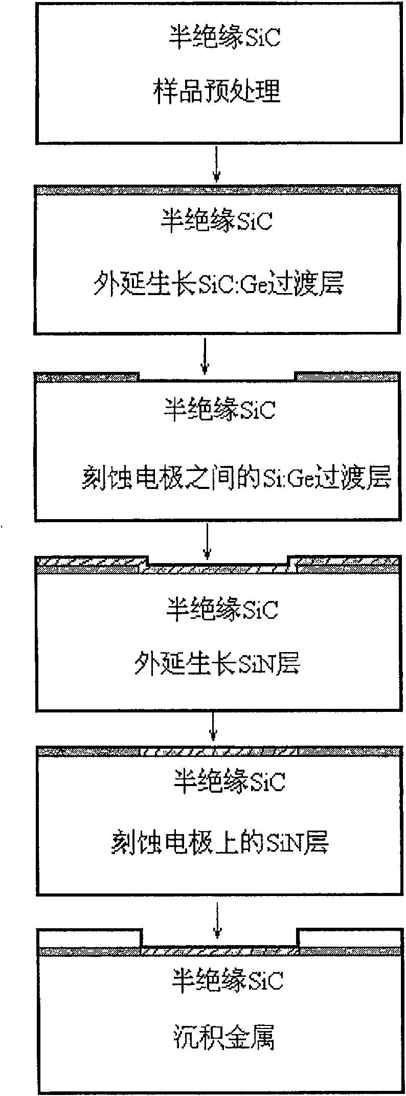
[0062] The steps of making the ohmic contact with the intermediate layer are basically the same as the scheme 2 of the embodiment 1, the only difference is that the optimal thickness of the epitaxial 3C-SiC:Ge in the step 2 is 180nm.
Embodiment 3
[0063] In Embodiment 3, a semi-insulating 6H-SiC photoconductive switch is taken as an example.
[0064] The steps of using the heavily doped layer to make its ohmic contact are the same as the scheme 1 of Example 1, the only difference is that in step 2, a p-type GaN heavily doped layer is used for the deep main compensation type semi-insulating 4H-SiC, and the doping dose is 3.75×10 19 , the optimal thickness of doping is 93.75nm; for deep donor compensated semi-insulating SiC, an n-type GaN heavily doped layer is used, and the doping dose is 3.56×10 19 , the optimum thickness of doping is 93.75nm.
[0065] The steps of making an ohmic contact with the intermediate layer are basically the same as the scheme 2 of the embodiment 1, the only difference is that the optimal thickness of the epitaxial 3C-SiC:Ge in the step 2 is 234nm.
PUM
 Abstract
Description
Claims
Application Information
 - R&D
- Intellectual Property
- Life Sciences
- Materials
- Tech Scout
- Unparalleled Data Quality
- Higher Quality Content
- 60% Fewer Hallucinations
Browse by: Latest US Patents, China's latest patents, Technical Efficacy Thesaurus, Application Domain, Technology Topic, Popular Technical Reports.
© 2025 PatSnap. All rights reserved.Legal|Privacy policy|Modern Slavery Act Transparency Statement|Sitemap|About US| Contact US: help@patsnap.com