A kind of transparent conductive film with enhanced thermal stability and its preparation method and application
A transparent conductive film, thermally stable technology
- Summary
- Abstract
- Description
- Claims
- Application Information
AI Technical Summary
Problems solved by technology
Method used
Image
Examples
Embodiment 1
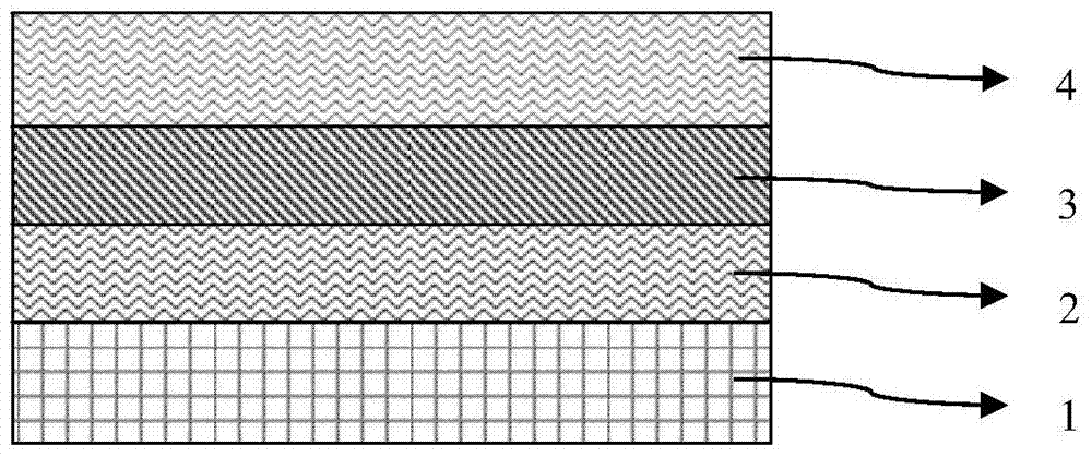
[0030] A kind of transparent conductive film based on silver alloy layer, its cross-sectional schematic diagram is as follows figure 1 As shown, it consists of a substrate 1, a first semiconductor layer 2, a silver alloy layer 3 and a second semiconductor layer 4 from bottom to top;
[0031] The material of the substrate 1 is glass with a thickness of 1mm;
[0032] The material of the first semiconductor layer 2 is GZO with a thickness of 40nm;
[0033] The material of the silver alloy layer 3 is silver (AgAl), and the thickness is 12nm;
[0034] The material of the second semiconductor layer 4 is GZO with a thickness of 50nm.
[0035] The above-mentioned preparation method of a transparent conductive film based on silver aluminum alloy layer, the specific steps are as follows:
[0036] Use cleaned transparent glass, place it in the cavity of the magnetron sputtering system, and evacuate it to a vacuum of 10 -5 Torr, followed by Ar gas, sputtering the first semiconductor l...
Embodiment 2
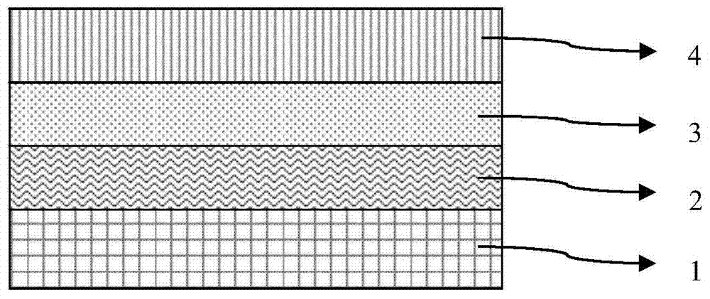
[0039]A kind of transparent conductive film based on silver alloy layer, its cross-sectional schematic diagram is as follows figure 2 As shown, it consists of a substrate 1 , a first semiconductor layer 2 , a silver alloy layer 3 and a second semiconductor layer 4 from bottom to top.
[0040] The material of the substrate 1 is glass with a thickness of 1mm;
[0041] The material of the first semiconductor layer 2 is MoO 3 , with a thickness of 10nm;
[0042] The material of the silver alloy layer 3 is AgAl with a thickness of 12nm;
[0043] The material of the second semiconductor layer 4 is MoO 3 , thickness 50nm.
[0044] The above-mentioned preparation method of a transparent conductive film based on silver aluminum alloy, the specific steps are as follows:
[0045] Use cleaned transparent glass, place it in the cavity of the vacuum thermal evaporation system, and evacuate it to a vacuum of 5*10 - 6 Torr, and then the first semiconductor layer MoO was plated respect...
Embodiment 3
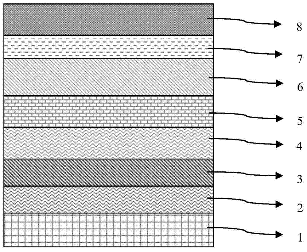
[0048] Such as image 3 As shown, the transparent conductive thin film structure obtained in Example 1 is applied to an organic solar cell, including 1 glass substrate, 2 first semiconductor layer GZO, 3 silver metal layer AgAl, 4 second semiconductor layer GZO, 5 Electron transport layer ZnO, 6 organic photoactive layers, 7 hole transport layer MoO 3 , 8 battery anode Ag. A single specific material is given in this embodiment, which does not limit the choice of other materials, but is just an example to illustrate the present invention. The transparent conductive film based on the silver-aluminum alloy layer is deposited by magnetron sputtering, then spin-coated with a 30nm ZnO electron transport layer 5, and after annealing at 140 degrees, then spin-coated with a PCE10:PC70BM (ratio 1:1.5) photoactive layer 6, followed by vacuum thermal evaporation of 8nm MoO 3 A hole transport layer 7 and an anode 8 of 100 nm silver layer. The efficiency of the organic solar cell adopti...
PUM
| Property | Measurement | Unit |
|---|---|---|
| thickness | aaaaa | aaaaa |
| thickness | aaaaa | aaaaa |
| thickness | aaaaa | aaaaa |
Abstract
Description
Claims
Application Information


