Plastic package device opening method

A device and component technology, applied in the field of unsealing electronic components, can solve problems such as low tolerance, and achieve the effect of improving the success rate and uniform corrosion rate

Active Publication Date: 2015-05-06
CASIC DEFENSE TECH RES & TEST CENT
View PDF5 Cites 32 Cited by
  • Summary
  • Abstract
  • Description
  • Claims
  • Application Information

AI Technical Summary

Problems solved by technology

The conventional method of unsealing can only acid-etch the limited area in the middle, usually the surrounding area is not completely exposed, but the middle area has been corroded, and a single corrosive liquid is used, which is likely to cause the lowest tolerance of components (such as inductors, resistors, etc.) Corrosion occurred first, such as figure 2 shown

Method used


Image

  • Plastic package device opening method
  • Plastic package device opening method
  • Plastic package device opening method

Examples


Embodiment 1

[0032] As an embodiment of the present invention, taking the LTM series plastic-encapsulated device of LINEAR company as an example, the method for unsealing the plastic-encapsulated device includes the following steps:

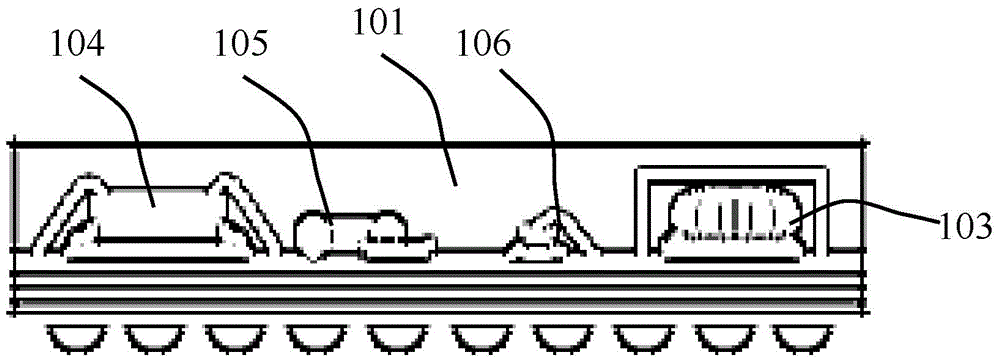
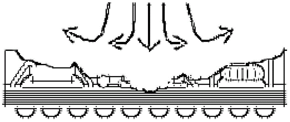
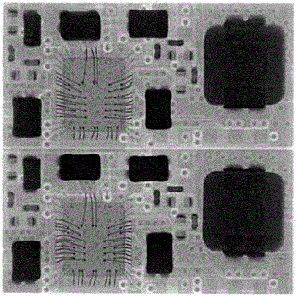
[0033] 1. Before opening the package, use the X-ray inspection method to locate the position and depth of each component and chip inside the plastic packaged device, and obtain the size, position and depth information of each component and chip inside the device, such as image 3 shown. Under normal circumstances, unpacking only needs to expose the internal chip, inductance and resistance and capacitance, so only the encapsulation material on the surface of these components and chips needs to be removed.

[0034] 2. According to the size, position and depth information of each element and chip inside the plastic-encapsulated device obtained in step 1, the plastic-encapsulated device is unsealed by laser ablation to remove the encapsulation material 101 on the...

Embodiment 2

[0043] As an embodiment of the present invention, taking the LTM series plastic-encapsulated device of LINEAR company as an example, the method for unsealing the plastic-encapsulated device includes the following steps:

[0044] 1. Before opening the package, use the X-ray inspection method to locate the position and depth of each component and chip inside the plastic packaged device, and obtain the size, position and depth information of each component and chip inside the device, such as image 3 shown. Under normal circumstances, unpacking only needs to expose the internal chip, inductance and resistance and capacitance, so only the encapsulation material on the surface of these components and chips needs to be removed.

[0045] 2. According to the size, position and depth information of each element and chip inside the plastic-encapsulated device obtained in step 1, the plastic-encapsulated device is unsealed by laser ablation to remove the encapsulation material 101 on the...

Embodiment 3

[0054] As an embodiment of the present invention, taking the LTM series plastic-encapsulated device of LINEAR company as an example, the method for unsealing the plastic-encapsulated device includes the following steps:

[0055] 1. Before opening the package, use the X-ray inspection method to locate the position and depth of each component and chip inside the plastic packaged device, and obtain the size, position and depth information of each component and chip inside the device, such as image 3 shown. Under normal circumstances, unpacking only needs to expose the internal chip, inductance and resistance and capacitance, so only the encapsulation material on the surface of these components and chips needs to be removed.

[0056] 2. According to the size, position and depth information of each element and chip inside the plastic-encapsulated device obtained in step 1, the plastic-encapsulated device is unsealed by laser ablation to remove the encapsulation material 101 on the...


PUM


Abstract

The invention discloses a plastic package device opening method. The plastic package device opening method comprises positioning the positions and the depths of various elements inside a plastic package device to obtain the size, position and depth information of the various elements and the chip inside the device; opening the plastic package device through a laser ablation method to remove package materials on the surface of the plastic package device to exactly expose internal lead bonding wires in a chip area, tin-lead solder spots adjacent to a resistance capacitor, and an inductor adjacent to the inductor; masking the ablated plastic package device to mask the area not requiring corrosion with aluminum foils, and performing local corrosion on the masked plastic package device through corrosives. The plastic package device opening method can help precisely control the opening depth of every local area of the plastic package device and the properties of the corrosives, achieve precise multi-spot and layer-by-layer opening control effects and well solve the problem that traditional methods cannot easily open plastic package mixed integrated circuits.

Description

technical field [0001] The invention relates to the technical field of unsealing of electronic components, in particular to a method for unsealing a plastic-sealed device. Background technique [0002] In failure analysis of semiconductor devices, the device needs to be unpacked to expose the internal chips or components for subsequent analysis. However, with the development of packaging technology and level, the packaging methods and processes of electronic components have undergone revolutionary progress, and multi-layer and hybrid packaging plastic packaging devices have appeared. The existing acid unsealing method has good universality for plastic packaged semiconductor devices with only one chip inside, but due to the poor directionality and controllability of acid unsealing, it is difficult for plastic packaged devices and multi-layer structures with multiple chips or components inside. It is impossible to precisely control the multi-point and layer-by-layer unsealing...

Claims


Application Information

Patent Timeline
Patent Type & Authority Applications(China)
IPC IPC(8): H01L21/50
CPCH01L2224/48091H01L2924/15311H01L2924/181H01L2924/19105H01L2924/00012H01L2924/00014H01L21/02
Inventor 王坦刘晓昱贺峤
Owner CASIC DEFENSE TECH RES & TEST CENT
Why Eureka
Try Eureka