Method for manufacturing active area of broadband spectrum indium arsenide/indium phosphide quantum dot laser

A technology of indium arsenide and indium quantum, which is applied in lasers, phonon exciters, laser components, etc., can solve the problems of low luminous efficiency of quantum dots and achieve good optical performance

Active Publication Date: 2015-05-06
INST OF SEMICONDUCTORS - CHINESE ACAD OF SCI
View PDF6 Cites 8 Cited by
  • Summary
  • Abstract
  • Description
  • Claims
  • Application Information

AI Technical Summary

Problems solved by technology

However, the small lattice mismatch between InAs and InP materials and the As / P interchange effect at the growth interface make the luminous efficiency of quantum dots low

Method used


Image

  • Method for manufacturing active area of broadband spectrum indium arsenide/indium phosphide quantum dot laser
  • Method for manufacturing active area of broadband spectrum indium arsenide/indium phosphide quantum dot laser
  • Method for manufacturing active area of broadband spectrum indium arsenide/indium phosphide quantum dot laser

Examples


Embodiment

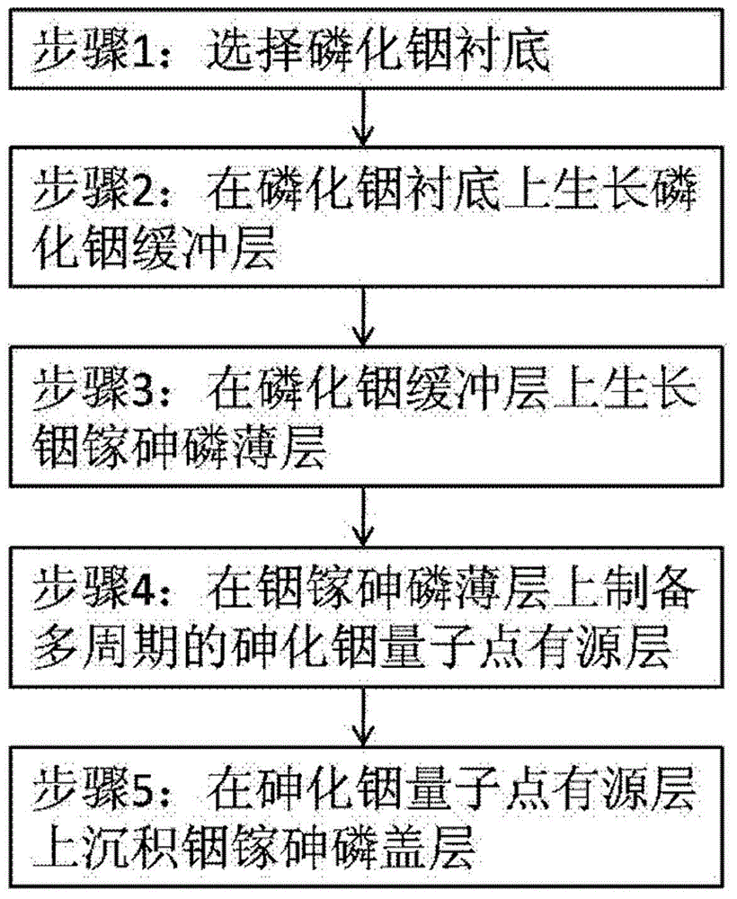
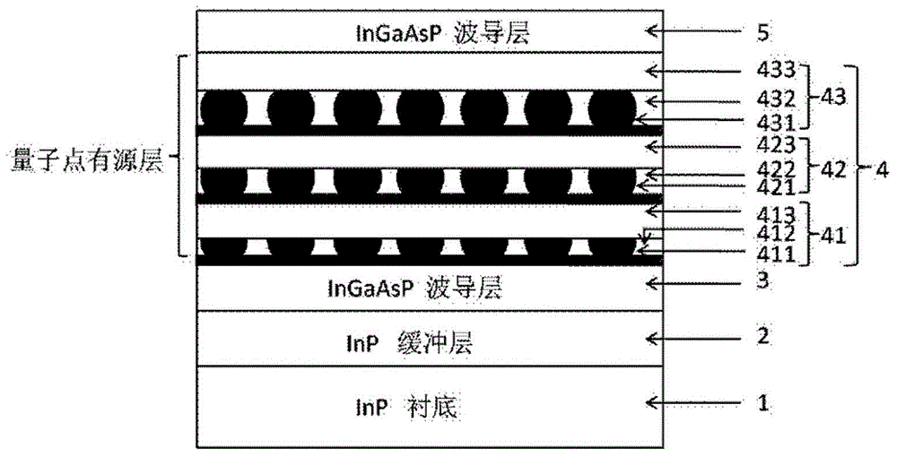
[0030] refer to figure 1 and figure 2 , a method for making an active region of a wide-spectrum indium arsenide / indium phosphide quantum dot laser, comprising the steps of:

[0031] Step 1: Select an indium phosphide substrate 1;

[0032] Step 2: growing an indium phosphide buffer layer 2 on the indium phosphide substrate 1; the growth temperature of the indium phosphide buffer layer 2 is 645°C; the growth thickness is 300nm, and the molar ratio of group V and group III sources is 200 ;

[0033] Step 3: growing a lattice-matched InGaAsP thin layer 3 on the InP buffer layer 2; the growth temperature of the InGaAsP thin layer 3 is 645°C, and its growth rate is 0.5nm / s, V The / III ratio was 150. This layer serves as the lower barrier layer of the active region;

[0034] Step 4: Prepare a multi-period indium arsenide quantum dot active layer 4 on the indium gallium arsenide phosphorus thin layer 3, the indium arsenide quantum dot active layer 4 includes three periods of indi...


PUM


Abstract

Disclosed is a method for manufacturing an active area of a broadband spectrum indium arsenide/indium phosphide quantum dot laser. The method for manufacturing the active area of the broadband spectrum indium arsenide/indium phosphide quantum dot laser includes following steps: step 1, selecting an indium phosphide substrate; step 2, growing an indium phosphide buffer layer on the indium phosphide substrate; step 3, growing an indium gallium arsenide phosphide thin layer with matched lattices on the indium phosphide buffer layer; step 4, preparing a polycyclic indium arsenide quantum dot active layer on the indium gallium arsenide phosphide thin layer, setting the indium gallium arsenide phosphide thin layer as a lower barrier layer of the indium arsenide quantum dot active layer; step 5, depositing an indium gallium arsenide phosphide cover layer on the indium arsenide quantum dot active layer, and setting the indium gallium arsenide phosphide cover layer as an upper barrier layer of the indium arsenide quantum dot active layer. The method for manufacturing the active area of the broadband spectrum indium arsenide/indium phosphide quantum dot laser regulates and controls the height of quantum dots by changing the thickness of the first cover layer, obtains different light wavelengths in different periods, and achieves good optical performance and luminescence spectrum larger than 300nm in width by enabling the polycyclic quantum dots to simultaneously emit light.

Description

technical field [0001] The invention belongs to the technical field of semiconductors, in particular to an epitaxial growth method for an active region of a wide-spectrum indium arsenide / indium phosphide quantum dot laser. Background technique [0002] Broad-spectrum laser sources have a very wide range of applications in precision spectral analysis, biomedicine, and environmental testing. In particular, a broad-spectrum laser source with an emission wavelength near 1.55 μm has a very important application prospect in the fields of dense wavelength division multiplexing and coherent optical communication. The self-organized semiconductor quantum dot material grown in the Stranski-Krastanov (SK) mode has a large non-uniform size distribution and a wider luminescent spectral bandwidth than the quantum well material. This makes the quantum dot material more suitable for use as an active region material for a wide-spectrum emitting laser source. In order to further increase th...

Claims


Application Information

Patent Timeline
Patent Type & Authority Applications(China)
IPC IPC(8): H01S5/343
Inventor 杨涛高凤罗帅季海铭
Owner INST OF SEMICONDUCTORS - CHINESE ACAD OF SCI
Why Eureka
Try Eureka