Ultra-narrow-pitch wafer level encapsulation cutting method

A wafer-level packaging and cutting method technology, which is applied in the fields of electrical components, semiconductor/solid-state device manufacturing, circuits, etc., can solve the problems affecting the number of packaged products, cutting process restrictions, and affecting the packaging yield, so as to improve the packaging yield , the process window is enlarged, and the process is simple

Active Publication Date: 2015-05-20
HUATIAN TECH KUNSHAN ELECTRONICS
View PDF6 Cites 13 Cited by
  • Summary
  • Abstract
  • Description
  • Claims
  • Application Information

AI Technical Summary

Problems solved by technology

If the dicing line is too wide, it will affect the number of packaged products; if the number of packaged products is to be increased, this cutting method cannot meet the requirements of wafers with narrow dicing lines. Cutting stress, affecting packaging yield
Therefore, the cutting process is limited

Method used


Image

  • Ultra-narrow-pitch wafer level encapsulation cutting method
  • Ultra-narrow-pitch wafer level encapsulation cutting method
  • Ultra-narrow-pitch wafer level encapsulation cutting method

Examples


Embodiment 1

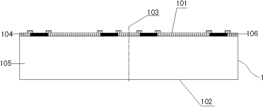
[0044] Figure 1 to Figure 8 A cross-sectional view of the manufacturing process of the ultra-narrow-pitch wafer-level packaging cutting method of the present invention is shown. Such as figure 1 As shown, a bare wafer 1 is provided, the functional surface thereof is the front side 101 , and the opposite side thereof is the back side 102 . The wafer includes a substrate 105 , a dielectric layer 104 on the functional surface of the substrate, and pads 106 partially disposed in the dielectric layer.

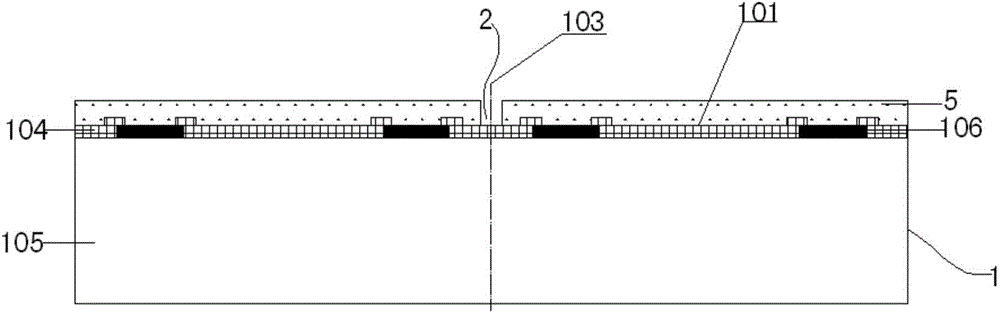
[0045] Next, if figure 2 As shown, a layer of photoresist 5 is coated on the front side of the wafer 1, and a first layer extending from the front side to the back side is formed on the front side of the wafer at a position facing the scribe line 103 through exposure and development processes. Opening 2, the first opening exposes the dielectric layer 104 facing the wafer dicing line;

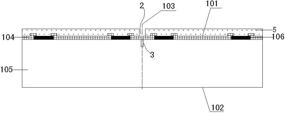
[0046] Next, if image 3 As shown, a second opening 3 extending from the front side to the ...

Embodiment 2

[0050] Figures 9 to 17 A cross-sectional view of a wafer-level packaging cutting process according to an embodiment of the present invention is shown. Such as Figure 9As shown, a half-encapsulated wafer 1 is provided, the functional surface of the wafer is a front surface 101, and the opposite side is a back surface 102, and the wafer includes a substrate 105, a dielectric layer 104 and a part of the functional surface of the substrate. The welding pad 106 arranged in the dielectric layer, the front side of the wafer is formed with a metal wiring layer 6 electrically leading out the welding pad 106 in the wafer dielectric layer, and a protective layer 7 is arranged above the metal wiring layer, A solder ball 8 serving as a connection window between the metal wiring layer and the outside world is formed on the protection layer, and the material of the protection layer is photoresist;

[0051] Next, if Figure 10 As shown, through the exposure and development process, the f...


PUM


Abstract

The invention discloses an ultra-narrow-pitch wafer level encapsulation cutting method. According to the method, a layer of photoresist is paved at the front side of a wafer, a first opening is formed through an exposure and development process, and a dielectric layer corresponding to a cutting path is exposed; then, a second opening is formed through an etching process or a laser cutting process, so that the second opening penetrates into a substrate at a certain depth; then, the grinding is carried out from the back surface, so that the stress is totally concentrated in a sharp corner position of the second opening formed through etching or cutting, and certain cracks are generated; if the extension resistance generated in the grinding process is great enough, the cracks can crack along a certain angle, and the wafer is further divided into single chips; if the extension resistance generated in the grinding process is not great enough, certain external force is exerted on a wafer, so that the cracks expand, and the water is further divided into the single chips. The ultra-narrow-pitch wafer level encapsulation cutting method has the advantages that the cutting of the wafer with the ultra-narrow cutting passage can be realized, in addition, the technological process is simple, and the process window is also correspondingly increased.

Description

technical field [0001] The invention relates to a cutting method for semiconductor packaging, in particular to an ultra-narrow-pitch wafer-level packaging cutting method. Background technique [0002] In wafer-level chip-scale packaging, after the packaging is completed, the entire wafer needs to be cut and separated into individual chips. In the prior art, the cutting process generally adopts mechanical cutting. Usually, the width of the dicing track is greater than the width of the cutting knife by more than 30 μm, and the minimum knife width is generally about 20 μm. Therefore, the narrowest dicing track also occupies a width greater than 50 μm. If the dicing line is too wide, it will affect the number of packaged products; if the number of packaged products is to be increased, this cutting method cannot meet the requirements of wafers with narrow dicing lines. Cutting stress affects packaging yield. Therefore, the cutting process is limited. Contents of the inventio...

Claims


Application Information

Patent Timeline
Patent Type & Authority Applications(China)
IPC IPC(8): H01L21/78
CPCH01L21/78
Inventor 万里兮杨力钱静娴翟玲玲黄小花沈建树王晔晔
Owner HUATIAN TECH KUNSHAN ELECTRONICS
Why Eureka
Try Eureka