Intelligent card module

A smart card and functional pad technology, applied in the field of smart card modules, can solve the problems of high production cost and storage cost of smart card modules, discharge of acid pollutants and waste water, inability to solder pads, etc., and achieve high environmental protection effect and low operating cost. The effect of low, continuous performance effect

Inactive Publication Date: 2015-05-20
上海安缔诺科技有限公司
View PDF5 Cites 5 Cited by
  • Summary
  • Abstract
  • Description
  • Claims
  • Application Information

AI Technical Summary

Problems solved by technology

Among them, the smart card carrier tape uses conventional copper-clad boards to etch to produce circuits, and then undergoes electroplating nickel and electroplating gold processes. During the process, a large amount of acid pollutants and waste water will be discharged, which will have a serious impact on the environment.
In addition, the traditional chip is mounted on the smart card carrier tape in the form of a bare chip. The bare chip needs to be used in a clean workshop environment and stored in a nitrogen environment. The production cost and storage cost of the module remain high

Method used


Image

  • Intelligent card module
  • Intelligent card module
  • Intelligent card module

Examples


Embodiment 1

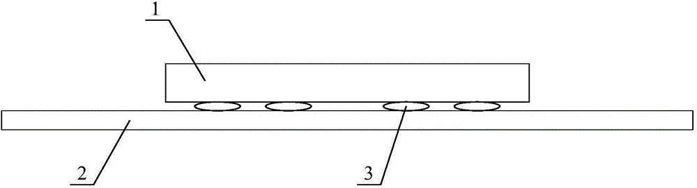
[0052] like image 3 As shown, a plurality of functional pads 14 of the chip 11 and a plurality of functional pads 15 of the carrier 12 are welded together in one-to-one correspondence, so that a plurality of functional pads 14 of the chip 11 and the carrier The multiple functional pads 15 of 12 are connected in one-to-one correspondence. The plurality of functional pads 15 of the carrier 12 are respectively provided with bump solder balls 18, and the plurality of functional solder pads 15 of the carrier 12 are welded with the carrier tape functional pads through the bump solder balls 18 respectively. together. Since the function of the bump solder balls 18 is to allow the plurality of functional pads 15 of the carrier 12 of the chip packaging module 1 to realize electrical conduction with the functional pads of the carrier tape 2, so the The material of the bump solder ball 18 should be a metal soldering material with better electrical conductivity; further, the material of...

Embodiment 2

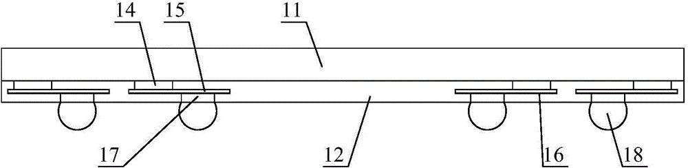
[0058] like Figure 4 As shown, the chip 11 is fixed on the carrier 12 by an adhesive 13 , and the multiple functional pads 14 of the chip 11 are respectively connected to the corresponding functional pads 15 of the carrier 12 through wires.

[0059] Then the manufacturing method of the smart card module of embodiment two is as follows:

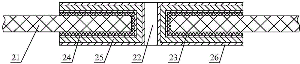
[0060] The making of carrier tape 2: same as embodiment one.

[0061] The making of chip packaging module 1: as Figure 4 As shown, the chip 11 is fixed on the carrier 12 with an adhesive 13; then the functional pads 14 of the chip 11 and the corresponding functional pads 15 of the carrier 12 are wire-bonded to make the chip A plurality of functional pads 14 of 11 are respectively connected to the corresponding functional pads 15 of the carrier 12 through wires; afterward, in order to make the chip 11 achieve high reliability in any use environment, after wire bonding The chip 11 and the carrier 12 are subjected to injection molding packag...


PUM


Abstract

The utility model provides an intelligent card module, comprising a carrier tape and a chip packaging module. The carrier tape comprises a carrier tape insulation base material with the panel provided with a plurality of through holes, wherein the inner wall of each through hole and two end surfaces of the peripheral carrier tape insulation base materials are all provided with a catalyzed printing ink line layer, and the outside of the catalyzed printing ink line layer is provided with a copper line layer to from carrier tape function pads and carrier tap pads of the carrier tap which are conductive; the chip packaging module comprise a chip and a carrier; the function pads of the chip are correspondingly conducting with the function pads of the carrier; the function pads of the carrier are correspondingly conducting with the function pads of the carrier tape. According to the utility model, the chip packaging module and the carrier tape are combined in a welding mode to form an intelligent card module; compared with an intelligent card module prepared by traditional process, the intelligent card module of the utility model has better environmental protection effect and simpler process and generates less waste materials and pollution in production process; in addition, the intelligent card module keeps the performance effect of a traditional intelligent card module, and meanwhile greatly reduces raw material cost, production cost and maintenance cost.

Description

technical field [0001] The invention relates to a packaging technology for microelectronic semiconductors and integrated circuits, in particular to a smart card module. Background technique [0002] With the continuous advancement of integrated circuit packaging technology, the integration level of integrated circuits is increasing day by day, the functions are becoming more and more abundant, and the requirements for product application fields are becoming more and more stringent, which requires integrated circuit packaging enterprises to develop new types of Package form to meet new requirements. [0003] For example, in the field of smart card packaging, the demand for smart cards in domestic and foreign markets is very large. At present, the smart card industry is developing towards the route of technological innovation. New technologies are constantly emerging, and new manufacturing technologies are also increasing. The technology is also continuously improved and stre...

Claims


Application Information

Patent Timeline
Patent Type & Authority Applications(China)
IPC IPC(8): H01L23/488
CPCH01L2224/32245H01L2224/45147H01L2224/45565H01L2224/48091H01L2224/48247H01L2224/73265H01L2924/00014H01L2924/00H01L2224/45655H01L2224/45644
Inventor 刘锋唐荣烨杨兆国
Owner 上海安缔诺科技有限公司
Why Eureka
Try Eureka