Organic light-emitting device and production method thereof

An electroluminescent device and luminescent technology, which is applied in the direction of organic light-emitting devices, organic light-emitting device structures, organic semiconductor devices, etc., can solve the problems of poor ability to isolate water and oxygen, reduced luminous efficiency, and low electron transfer rate

Inactive Publication Date: 2015-05-20
OCEANS KING LIGHTING SCI&TECH CO LTD +2
View PDF0 Cites 0 Cited by
  • Summary
  • Abstract
  • Description
  • Claims
  • Application Information

AI Technical Summary

Problems solved by technology

[0003] However, in the existing organic electroluminescent devices, the electron injection layer is one of the important functional layers. During the manufacturing process, due to the poor ability of the material selected for the electron injection layer to isolate water and oxygen, water vapor will penetrate through cracks and affect Ele

Method used


Image

  • Organic light-emitting device and production method thereof
  • Organic light-emitting device and production method thereof

Examples


preparation example Construction

[0031] The method for preparing the above-mentioned organic electroluminescent device specifically includes the following steps:

[0032] 1. Rinse the glass with distilled water and ethanol, and soak it in isopropanol overnight.

[0033] 2. Prepare a conductive anode film on the glass cleaned in the above steps to obtain an anode conductive substrate, and then vapor-deposit sequentially on the anode conductive substrate to prepare a hole injection layer, a hole transport layer, a light-emitting layer, and an electron transport layer.

[0034] 3. Next, an electron injection layer is prepared on the above electron transport layer, and the electron injection layer is composed of a rubidium compound doped layer and an iron salt layer.

[0035] The rubidium compound doped layer is deposited by thermal resistance evaporation, which is composed of rubidium compound, metal with low work function and metal with high work function, and has a thickness of 30-100 nm. The material of the ...

Embodiment 1

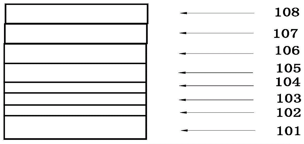
[0049] Such as figure 1 As shown, the organic electroluminescent device in this embodiment is a layered structure, and each layer is in turn:

[0050] Anode conductive substrate 101 of glass / IZO, MoO 3 The hole injection layer 102 of material, the hole transport layer 103 of TAPC material, the light-emitting layer 104 of ADN material, the electron transport layer 105 of TPBI material, Rb 2 CO 3 : Rubidium compound doped layer 106 of Ca:Ag material, FeCl 3 The iron salt layer 107 made of Ag material and the cathode layer 108 made of Ag material. The rubidium compound doped layer 106 and the iron salt layer 107 constitute an electron injection layer. (where the slash " / " indicates a layered structure, and the colon ":" indicates mutual doping)

[0051] The above-mentioned organic electroluminescent device is prepared according to the following steps in sequence:

[0052] 1. Rinse the glass with distilled water and ethanol, and soak it in isopropanol overnight.

[0053] 2....

Embodiment 2

[0064] The layered structure of the organic electroluminescent device of the following examples 2-4 is basically the same as that of the example 1, so no illustration will be given here.

[0065] The organic electroluminescent device in this embodiment is a layered structure, and each layer is sequentially:

[0066] Anode conductive substrate of glass / IZO, V 2 o 5 Hole injection layer made of NPB material, hole transport layer made of NPB material, light emitting layer made of DCJTB material, electron transport layer made of TPBi material, rubidium compound doped layer made of RbCl:Mg:Au material, FeBr 3 The iron salt layer made of Al material and the cathode layer made of Al material. The rubidium compound doped layer and the iron salt layer 107 constitute an electron injection layer. (where the slash " / " indicates a layered structure, and the colon ":" indicates mutual doping)

[0067] The above-mentioned organic electroluminescent device is prepared according to the fol...


PUM

PropertyMeasurementUnit
Work functionaaaaaaaaaa
Thicknessaaaaaaaaaa
Thicknessaaaaaaaaaa

Abstract

The invention relates to an organic light-emitting device and a production method thereof. The organic light-emitting device comprises an anode conducting substrate, a hole injection layer, a hole transmission layer, a light-emitting layer, an electron transmission layer, an electron injection layer and a cathode layer which are stacked in sequence; the electron injection layer comprises a rubidium compound doping layer and an iron salt layer; the rubidium compound doping layer is made of materials of a rubidium compound, low-work function metal and high-work function metal; the rubidium compound is made of materials of rubidium carbonate, rubidium chloride, rubidium nitrate or rubidium sulfate. The rubidium compound of the organic light-emitting device is low in melting point and easy to evaporate and plate; due to existing of metal ions, work function is low, an electronic injection barrier between the electron transmission layer and the injection layer can be reduced, and injection of the electron is benefited.

Description

technical field [0001] The invention relates to the field of optoelectronic devices, in particular to an organic electroluminescent device. The invention also relates to a preparation method of the organic electroluminescent device. Background technique [0002] In 1987, C.W.Tang and Van Slyke of Eastman Kodak Company in the United States reported a breakthrough in the research of organic electroluminescence. A high-brightness, high-efficiency double-layer organic electroluminescent device (OLED) was fabricated using ultra-thin film technology, and its brightness reached 1000cd / m at 10V 2 , its luminous efficiency is 1.51lm / W, and its lifespan is more than 100 hours. [0003] However, in the existing organic electroluminescent devices, the electron injection layer is one of the important functional layers. During the manufacturing process, due to the poor ability of the material selected for the electron injection layer to isolate water and oxygen, water vapor will penetra...

Claims


Application Information

Patent Timeline
IPC IPC(8): H01L51/50H01L51/54H01L51/56
CPCH10K50/171H10K2102/00H10K2102/302H10K71/00
Inventor 周明杰黄辉张振华王平
Owner OCEANS KING LIGHTING SCI&TECH CO LTD
Why Eureka
Try Eureka