

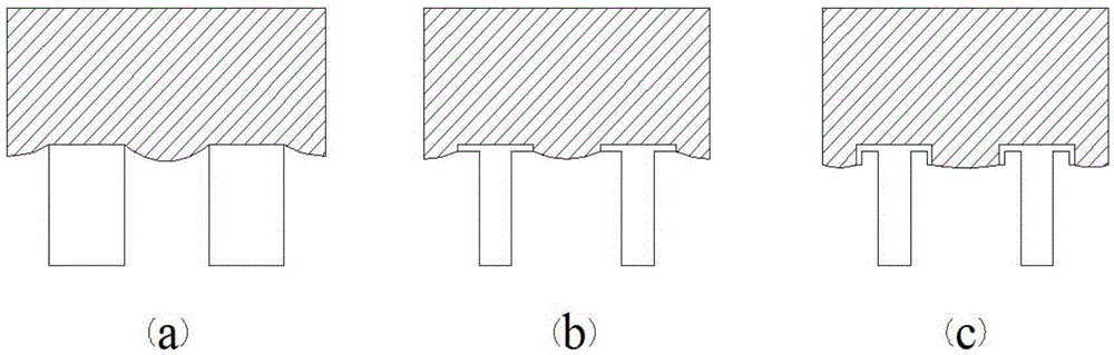
A kind of preparation method of superhydrophobic reentrant t-shaped microcolumn structure
A super-hydrophobic and micro-column technology, which is applied in the direction of microstructure technology, microstructure devices, and manufacturing microstructure devices, can solve the problems of difficult process, complex process, expensive equipment, etc. The effect of speeding up the fill rate
- Summary
- Abstract
- Description
- Claims
- Application Information
AI Technical Summary
Problems solved by technology
Method used
Image

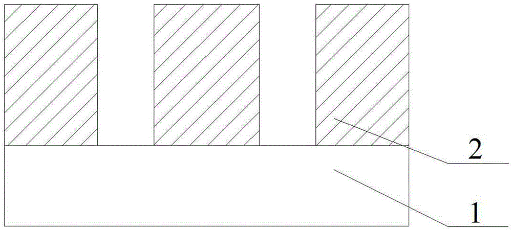
Examples
Embodiment 1
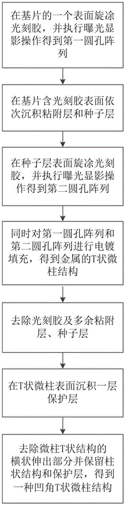
[0046] The technical scheme of the present embodiment 1 can be specifically implemented through the following steps:
[0047] Step 1, photolithography
[0048] Spin-coat NR26-25000P negative photoresist on a clean substrate with a thickness of 20 μm; use a mask with a circular array pattern, the circular area is opaque, the diameter of the circle is 10 μm, and the spacing is 30 μm; use MA6 contact photoresist engraving machine.
[0049] Step 2, developing
[0050] Put the substrate after step 1 into RD6 developing solution for development, and obtain the first circular hole array structure of photoresist on the substrate.
[0051] Step 3, Magnetron Sputtering
[0052] The substrate with the photoresist circular hole array structure after development in the second step is deposited with the magnetron sputtering method to sequentially deposit the adhesion layer Ti and the seed layer Cu, and the thickness of Ti / Cu is 10nm / 50nm.
[0053] Step 4, photolithography
[0054] Spin...
Embodiment 2
[0066] The technical scheme of present embodiment 2 can be specifically implemented through the following steps:
[0067] Step 1, photolithography
[0068] Spin-coat NR26-25000P negative photoresist on a clean substrate with a thickness of 20 μm; use a mask with a circular array pattern, the circular area is transparent, the diameter of the circle is 10 μm, and the spacing is 100 μm; use MA6 contact photolithography machine.
[0069] Step 2, developing
[0070] Put the substrate after step 1 into RD6 developing solution for development, and obtain the first circular hole array structure of photoresist on the substrate.
[0071] Step 3, Magnetron Sputtering
[0072] The substrate with the photoresist circular hole array structure after development in the second step is deposited with an adhesion layer Ti and a seed layer Cu in sequence by magnetron sputtering, and the thickness of Ti / Cu is 10 / 50nm.
[0073] Step 4, photolithography
[0074] Spin-coat PR1-1000A positive pho...
Embodiment 3
[0088] The technical scheme of present embodiment 3 can be specifically implemented through the following steps:
[0089] Step 1, photolithography
[0090] Spin-coat NR26-25000P negative photoresist on a clean substrate with a thickness of 60 μm; use a mask with a circular array pattern, the circular area is transparent, the diameter of the circle is 20 μm, and the spacing is 120 μm; use MA6 contact photolithography machine.
[0091] Step 2, developing
[0092] Put the substrate after step 1 into RD6 developing solution for development, and obtain the first circular hole array structure of photoresist on the substrate.
[0093] Step 3, Magnetron Sputtering
[0094] On the substrate with the photoresist circular hole array structure developed in the second step, the adhesion layer Ti and the seed layer Cu are sequentially deposited by magnetron sputtering, and the thickness of Ti / Cu is 50 / 100nm.
[0095] Step 4, photolithography
[0096]Spin-coat PR1-4000A positive photore...
PUM
| Property | Measurement | Unit |
|---|---|---|
| thickness | aaaaa | aaaaa |
| thickness | aaaaa | aaaaa |
| thickness | aaaaa | aaaaa |
Abstract
Description
Claims
Application Information