A semiconductor structure with redistribution layer and its manufacturing method

A technology for rewiring layers and manufacturing methods, applied in semiconductor/solid-state device manufacturing, semiconductor devices, semiconductor/solid-state device components, etc., can solve problems such as complex manufacturing process, lower production cost, poor adhesion, etc., to achieve The effect of reducing production cost, reducing manufacturing process, and reducing layout flexibility

Active Publication Date: 2017-02-22
SILERGY SEMICON TECH (HANGZHOU) CO LTD
View PDF4 Cites 0 Cited by
  • Summary
  • Abstract
  • Description
  • Claims
  • Application Information

AI Technical Summary

Problems solved by technology

[0004] However, in the manufacturing method of this kind of semiconductor with rewiring structure in the prior art, in order to reduce material cost, copper material is usually selected to form the RDL layer, and copper is a hard metal, and its adhesion is not good, so in After forming the RDL layer, at least two laminated metal layers must be formed successively on the RDL layer (for example, the first metal layer is Ni, the second metal layer is Au or Pd, etc.) to increase the adhesion to the leads
Therefore, the manufacturing process of the rewiring structure on the chip surface of the prior art is complicated, which is not conducive to reducing the production cost.

Method used


Image

  • A semiconductor structure with redistribution layer and its manufacturing method
  • A semiconductor structure with redistribution layer and its manufacturing method
  • A semiconductor structure with redistribution layer and its manufacturing method

Examples


Embodiment Construction

[0026] Hereinafter, the present invention will be described in more detail with reference to the accompanying drawings. In the various figures, identical elements are indicated with similar reference numerals. For the sake of clarity, various parts in the drawings have not been drawn to scale. Also, some well-known parts may not be shown. For simplicity, the structure obtained after several steps can be described in one figure. In the following, many specific details of the present invention are described, such as device structures, materials, dimensions, processing techniques and techniques, for a clearer understanding of the present invention. However, the invention may be practiced without these specific details, as will be understood by those skilled in the art.

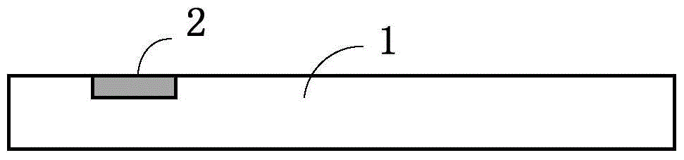
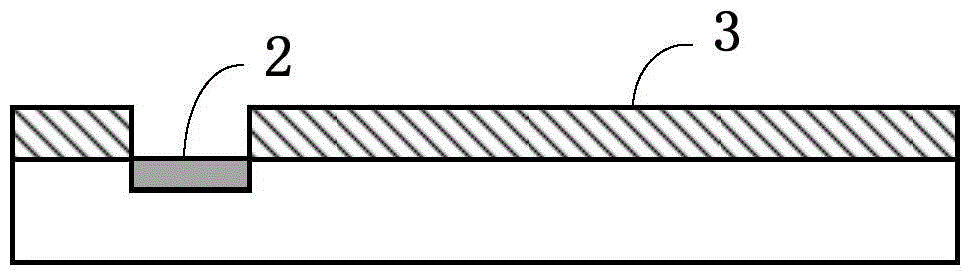
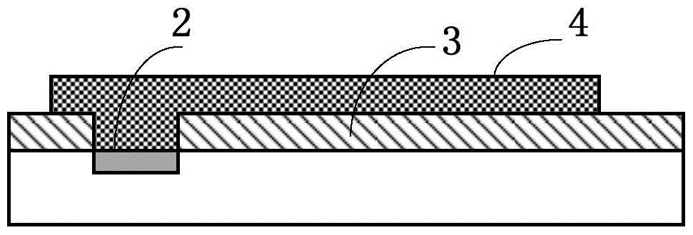
[0027] Figure 2a-2d are cross-sectional views of various stages of a method of fabricating a semiconductor structure with a redistribution layer according to an embodiment of the present invention.

[0028]...


PUM


Abstract

The invention discloses a semiconductor structure with a heavy wiring layer and a manufacturing method thereof. The semiconductor structure with the heavy wiring layer comprises a chip with an active surface, a first connecting pad and a second connecting pad which are positioned on the active surface, a passivation layer positioned on the active surface, and the heavy wiring layer positioned on the passivation layer, wherein the heavy wiring layer is electrically connected with the first connecting pad and the second connecting pad which are used for educing electrodes of an element inside the chip, and a part of the second connecting pad is exposed as an interconnecting welding area for achieving interconnection with the outside so as to enable an interconnecting welding area originally at the first connecting pad of the chip to be rearranged at the exposed second connecting pad and directly used as the interconnecting welding area, so that the integration degree and the layout flexibility of the chip are improved and the interconnecting resistance during chip packaging is reduced; the semiconductor structure with the heavy wiring layer is relatively simple, so that reduction in manufacturing processes and reduction in production cost are facilitated.

Description

technical field [0001] The invention relates to the technical field of chip packaging, in particular to a semiconductor structure with a rewiring layer and a manufacturing method thereof. Background technique [0002] The method of using wires to interconnect the pads on the semiconductor bare chip (die) and the corresponding pins of the lead frame has become the main process method for chip interconnection due to its low cost, high reliability and high yield. However, when the method of wire bonding is used to realize chip interconnection, it may be necessary to use a longer lead wire to realize the electrical connection between the pad and the pin due to the long distance between the pad and the corresponding pin, resulting in a large interaction. The problem of connecting resistance may also be that the welding area is blocked by other devices (such as inductors) above it, and the electrical connection with the corresponding pin cannot be realized through the lead wire. ...

Claims


Application Information

Patent Timeline
Patent Type & Authority Patents(China)
IPC IPC(8): H01L23/525H01L23/528H01L21/768
CPCH01L2224/05H01L2224/48091H01L2224/48247H01L2224/73265H01L2924/00014
Inventor 叶佳明
Owner SILERGY SEMICON TECH (HANGZHOU) CO LTD
Why Eureka
Try Eureka